Programming Model
http://www.motorola.com/computer/literature 1-7
1
Notes
1. Programmable via Falcon chipset.
2. To enable the Processor-hole area, program the Falcon chipset to
ignore 0x000A0000 - 0x000BFFFF address range and program the
Raven to map this address range to PCI memory space.
3. Programmable via Raven ASIC.
4. CHRP requires the starting address for the PCI memory space to be
256MB-aligned.
5. Programmable via Raven ASIC for either contiguous or spread-I/O
mode.
6. The first 1MB of ROM/FLASH Bank A appears at this range after
a reset if the rom_b_rv control bit is cleared. If the rom_b_rv
control bit is set then this address range maps to ROM/FLASH Bank
B.
7. The only method to generate a PCI Interrupt Acknowledge cycle
(8259 IACK) is to perform a read access to the Raven’s PIACK
register at 0xFEFF0030.
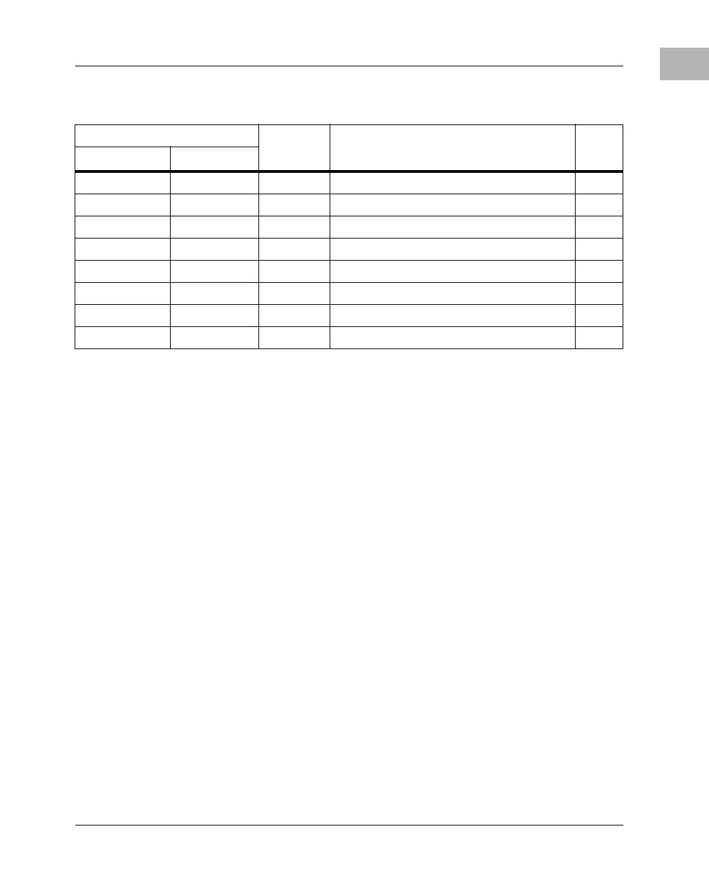
FE80 0000 FEF7 FFFF 7.5M Reserved
FEF8 0000 FEF8 FFFF 64K Falcon Registers
FEF9 0000 FEFE FFFF 384K Reserved
FEFF 0000 FEFF FFFF 64K Raven Registers 7
FF00 0000 FF7F FFFF 4M ROM/FLASH Bank A 1,6
FF80 0000 FF8F FFFF 1M ROM/FLASH Bank B 1,6
FF50 0000 FFEF FFFF 6M Reserved
FFF0 0000 FFFF FFFF 1M ROM/FLASH Bank A or Bank B 6
Table 1-3. CHRP Memory Map Example (Continued)
Processor Address Size Definition
Notes
Start End
 Loading...