Programming Model
http://www.motorola.com/computer/literature 1-19
1
all RAM configuration information is contained in the SPD data; fields
M_FREF and M_SPD [0:1} in the memory configuration register are not
used. This 32-bit read-only Register is defined as follows:
M_FREF Not used
M_SPD[0:1] Not used
R_A/B_TYP[0:1] ROM/Flash Type. This field is encoded as follows:
Note The device width is different from the width of the FLASH bank.
If the bank width is 64-bit and the device width is 16-bit then the
FLASH bank consists of four FLASH devices.
FLSHP[0:2] Bank A Flash memory size. This field is encoded as follows:
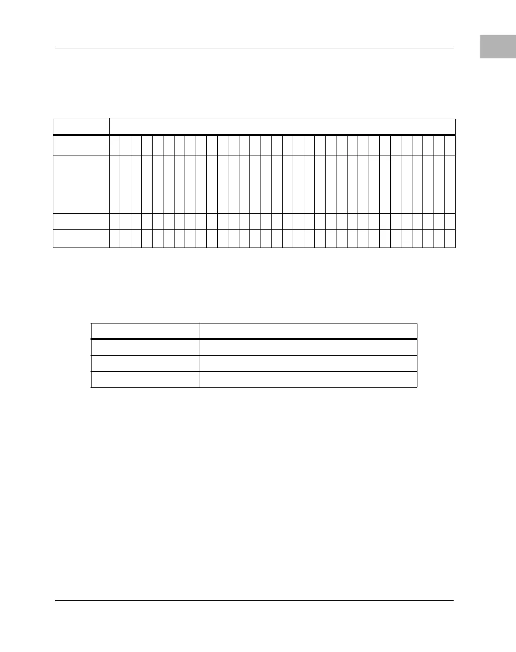
Register Memory Configuration Register - $FEF80404
Bit
32
33
34
35
36
37
38
39
40
41
42
43
44
45
46
47
48
49
50
51
52
53
54
55
56
57
58
59
60
61
62
63
Field
M_FREF
M_SPD0
M_SPD1
R_A_TYP0
R_A_TYP1
R_A_TYP2
R_B_TYP0
R_B_TYP1
R_B_TYP2
FLSHP0_
FLSHP1_
FLSHP2_
Operation
Reset
1
1
1
X
1
1
X
X
1
X
X
X
1
X
X
X
1
1
1
1
1
1
1
1
1
1
X
X
X
1
1
1
ROM_A/B_TYP[0:2] ROM/FLASH Type
0b000 to 0b101 Reserved
0b110
Intel
0b111
Unknown type (that is, ROM/FLASH Sockets)
 Loading...


