Section 1 Overview
Rev. 7.00 Mar 10, 2005 page 16 of 652
REJ09B0042-0700
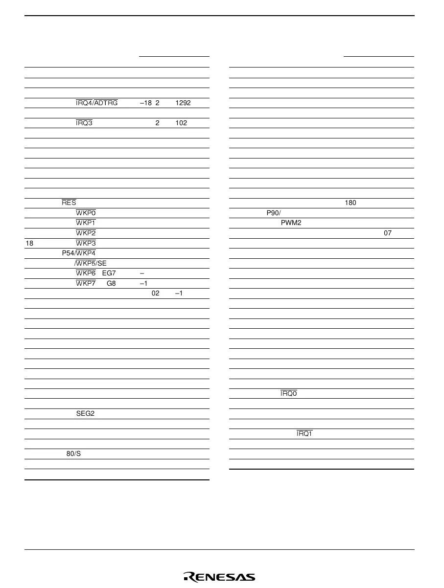
Table 1.3 Bonding Pad Coordinates of HCD64F38024, HCD64F38024R
Coordinates Coordinates
Pad No. Pad Name X (µ
µµ
µm) Y (µ
µµ
µm) Pad No. Pad Name X (µ
µµ
µm) Y (µ
µµ
µm)
1 PB7/AN7 –1802 1904 42 P83/SEG28 1802 –1898
2AV
CC
–1802 1717 43 P84/SEG29 1802 –1750
3 P13/TMIG –1802 1443 44 P85/SEG30 1802 –1594
4 P14/
IRQ4
/
ADTRG
–1802 1292 45 P86/SEG31 1802 –1454
5 P16 –1802 1157 46 P87/SEG32 1802 –1296
6 P17/
IRQ3
/TMIF –1802 1022 47 PA3/COM4 1802 –1182
7 X1 –1802 887 48 PA2/COM3 1802 –1068
8 X2 –1802 753 49 PA1/COM2 1802 –954
9AV
SS
–1802 638 50 PA0/COM1 1802 –840
10 V
SS
–1802 473 51 V3 1802 –726
11 OSC2 –1802 318 52 V2 1802 –534
12 OSC1 –1802 202 53 V1 1802 –402
13 TEST –1802 69 54 V
CC
1802 –267
14
RES
–1802 –63 55 V
SS
1802 –126
15 P50/
WKP0
/SEG1 –1802 –195 56 P90/PWM1 1802 206
16 P51/
WKP1
/SEG2 –1802 –355 57 P91/PWM2 1802 457
17 P52/
WKP2
/SEG3 –1802 –514 58 P92 1802 707
18 P53/
WKP3
/SEG4 –1802 –674 59 P93 1802 958
19 P54/
WKP4
/SEG5 –1802 –844 60 P94 1802 1209
20 P55/
WKP5
/SEG6 –1802 –1008 61 P95 1802 1460
21 P56/
WKP6
/SEG7 –1802 –1348 62 IRQAEC 1802 1710
22 P57/
WKP7
/SEG8 –1802 –1709 63 P30/UD 1802 1904
23 P60/SEG9 –1802 –1904 64 P31/TMOFL 1686 1999
24 P61/SEG10 –1686 –1999 65 P32/TMOFH 1222 1999
25 P62/SEG11 –1198 –1999 66 P33 1077 1999
26 P63/SEG12 –1057 –1999 67 P34 932 1999
27 P64/SEG13 –916 –1999 68 P35 788 1999
28 P65/SEG14 –755 –1999 69 P36/AEVH 643 1999
29 P66/SEG15 –625 –1999 70 P37/AEVL 498 1999
30 P67/SEG16 –493 –1999 71 P40/SCK32 353 1999
31 P70/SEG17 –352 –1999 72 P41/RXD32 226 1999
32 P71/SEG18 –202 –1999 73 P42/TXD32 63 1999
33 P72/SEG19 –69 –1999 74 P43/
IRQ0
–82 1999
34 P73/SEG20 72 –1999 75 PB0/AN0 –229 1999
35 P74/SEG21 213 –1999 76 PB1/AN1 –404 1999
36 P75/SEG22 330 –1999 77 PB2/AN2 –577 1999
37 P76/SEG23 459 –1999 78 PB3/AN3/
IRQ1
/TMIC –751 1999
38 P77/SEG24 583 –1999 79 PB4/AN4 –925 1999
39 P80/SEG25 730 –1999 80 PB5/AN5 –1099 1999
40 P81/SEG26 937 –1999 81 PB6/AN6 –1686 1999
41 P82/SEG27 1686 –1999
Note: V
SS
Pads (No. 9 and 10) should be connected to power supply lines.
TEST Pad (No. 13) should be connected to V
SS
.
If the pad of these aren’t connected to the power supply line, the LSI will not operate correctly. These values show the
coordinates of the centers of pads. The accuracy is ±5 µm. The home-point position is the chip’s center and the center
is located at half the distance between the upper and lower pads and left and right pads.
 Loading...


