5-30 srellortnoC evirD 30EVIRDOCE610-3.**CKD 30EVIRDOCE
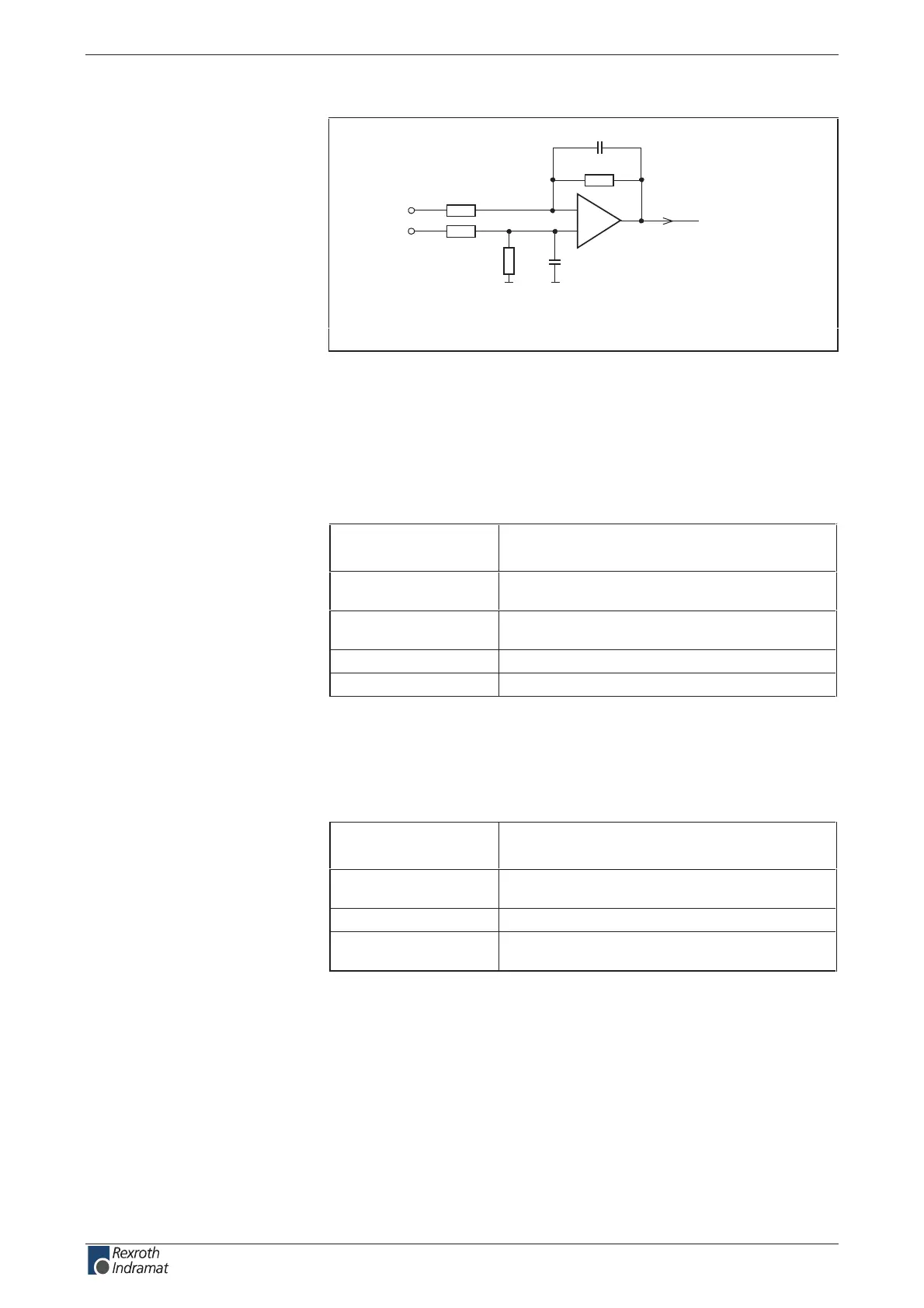
Input circuit G1Sin+ (S3), G1Sin- (S1):
AP5296F1.FH7
R1
R4
R2
R3
-
+
E+
E-
C2
C1
Schematics
R1: 4k
R2: 4k
R3: 8k25
R4: 8k25
C1: no data
C2: no data
Fig. 5-48: Input circuit
Features of the dierential input circuit G1Sin+ (S3), G1Sin- (S1):
Resolver
max. allowed amplitude
encoder signal
9,0 Vss
Evaluation
AD converter
12 Bit
--ycneuqerf timiL
%5 ± k8ecnatsiser tupnI
Fig. 5-49: Features of the dierential input circuit
see G1Sin+ (S3), G1Sin- (S1)
Features of the encoder output amplier stage G1_8V/Sin:
Resolver
ssV 2,81egatlov tuptuO
(sine with 4 kHz)
.ffe Am 07 CAtnerruc tuptuo .xam
min. D.C.
resistance of the load
35 R
Fig. 5-50: Features of the encoder output amplier stage
G1Sin+ (S3), G1Sin- (S1):
G1Cos+ (S4), G1Cos- (S2):
G1_8V/Sin:
customerservice@hyperdynesystems.com | (479) 422-0390
 Loading...