RFL 9780 RFL Electronics Inc.
November 1, 2000 8-5 (973) 334-3100
8.3.4 OUTPUT POWER ADJUSTMENT
The output of the filter is sent into an adjustable gain stage formed by U3A. This varies the output
level, which determines the system transmission power (10W, 3W or 1W output of the power amplifier
stage). Potentiometer R23 adjusts the nominal output voltage of the transmitter. It is set to achieve 10W
output with switches U6A, U6B and U6C open. In systems which require a “reserve” 1\10
th
power
output, U6A may be closed to attenuate the output signal to achieve the reduced power. This power
reduction can be varied by R18 if jumper J2 is in the “VAR” position. If analog switch U6C is closed,
the output power will drop to 3W. If both U6B and U6C are closed, the output power will drop to 1W.
All module functions are controlled by Field Programmable Gate Array (FPGA) U7. The FPGA reads
the on board configuration switches and control signals coming from other modules, and controls the
local hardware and indicators. It also computes the phase step required to generate the desired output
frequency.
8.4 CONTROLS AND INDICATORS
Figure 8-4 shows the locations of all controls and indicators on the transmitter module. These controls
and indicators are described in Table 8-1. LEDs DS1 through DS9 are visible with the module installed
in the chassis. All other controls are only accessible when the module is removed from the chassis or is
on a card extender.
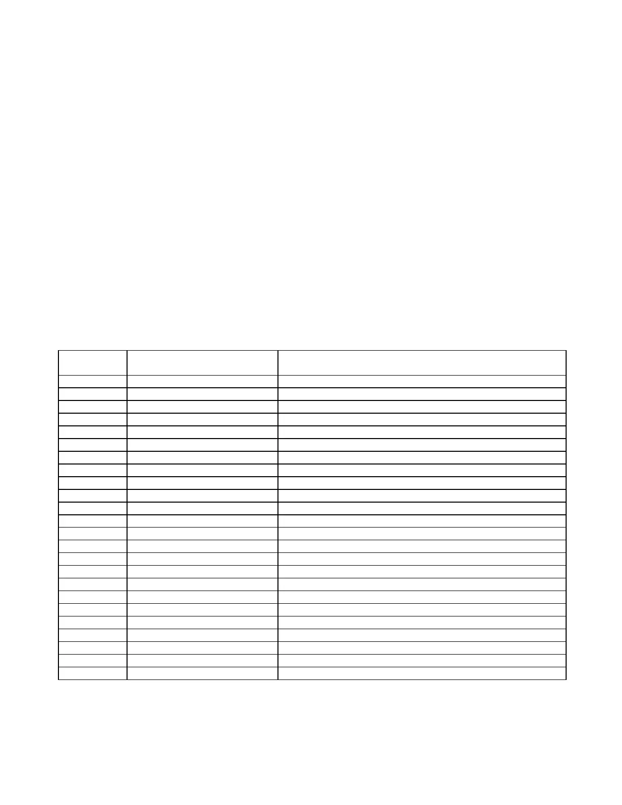
Table 8-1. Controls and Indicators, RFL 9780 Transmitter Module
Component
Designator
Name/
Description
Function
DS1 Carrier Enabled LED Indicates the carrier is being generated
DS2 Frequency 3 LED The carrier is set for a shift up frequency
DS3 Frequency 2 LED The carrier is set for a center frequency
DS4 Frequency 1 LED The carrier is set for a shift down frequency
DS5 Power 3 LED The system’s output power is 10W
DS6 Power 2 LED The system’s output power is 3W
DS7 Power 1 LED The system’s output power is 1W
DS8 Reserve LED The system is transmitting at reserve power (1/10 of normal power)
DS9 Voice Enabled LED The voice signal is being AM modulated onto the carrier
J1 Test Connector For factory use only
J2 Reserve level jumper Variable or fixed
R18 Potentiometer Used to vary the reserve level
R23 Potentiometer Sets the module’s nominal output level
SW1-SW2 Switch bank for shift down freq. Sets the desired shift down frequency
SW3-SW7 Switch bank for center frequency Sets the desired center frequency
SW8-SW9 Switch bank for shift up freq. Sets the desired shift up frequency
TP1 Test point Digital ground
TP2 Test point Signal ground
TP3 Test point Oscillator out (Output of DDS following filter)
TP4 Test point Carrier out (Final output of module)
TP5 Test point Voice in (Audio input signal in systems having the voice option)
TP6 Test point Reference
TP7 Test point +5Vdc (Digital)
TP8 Test point +5Vdc (Analog)