RFL 9780 RFL Electronics Inc.
April 8, 2003 19-5 (973) 334-3100
To protect the 5 Vdc output from excessive output currents, the voltage across shunt R26 is monitored
between pins 2 and 3 of U3. Like the voltage feedback path, exceeding limits, established by resistors
R35 and R36, causes pin 14 to go high and reduces the output voltage.
Integrated circuits U6, U7, and U8 are series regulators which provide post regulation for the secondary
outputs. Post regulation is required to meet the voltage regulation requirements of the supply.
Feedback for regulator U7 is provided by resistors R47, R25, potentiometer R49, and CR16. Feedback
paths for the other regulators are similarly structured.
All outputs have or’ing diodes. These diodes; CR12, CR15, CR18, CR19, allow two supplies to be
connected in parallel. Feedback signals for all outputs are taken before the or’ing diodes. The
temperature voltage sensitivities introduced by the or’ing diodes are compensated with diodes CR13,
CR16, CR17, and CR6.
19.2.3 CONTROLS AND INDICATORS
Figure 19-2 shows the location of all controls and indicators on the RFL 9780 Power supply module.
These controls and indicators are described in Table 19-2. DS1 is visible with the RFL 9780 Power
supply module installed in the chassis. All other controls and test points are only accessible when the
module is removed from the chassis or is on a card extender.
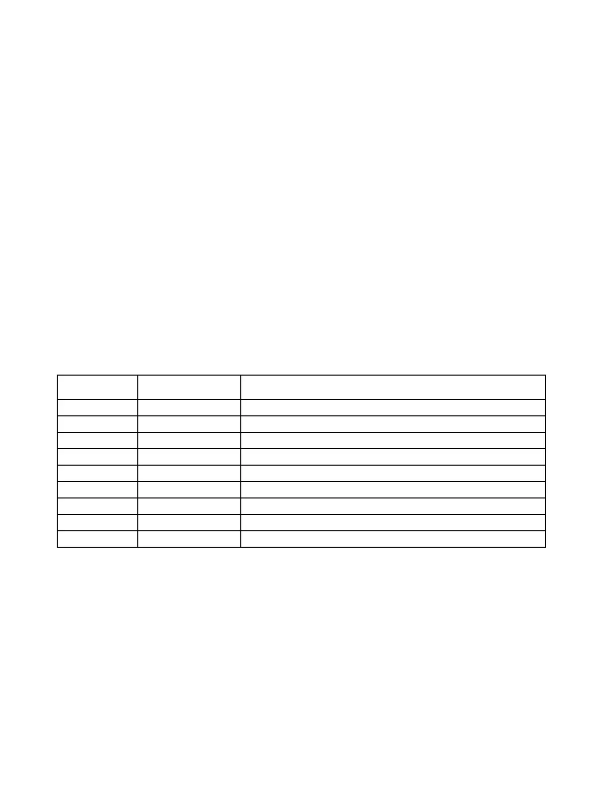
Table 19-2. Controls and indicators, RFL 9780 power supply module
Component
Designator
Name/
Description
Function
DS1 LED indicator (green) ON/OFF power indicator
R44 Potentiometer +5 Vdc adjust (for factory use only)
R49 Potentiometer +15 Vdc adjust (for factory use only)
R50 Potentiometer -15 Vdc adjust (for factory use only)
TP1 Test point Power supply common
TP2 Test point +5 Vdc
TP3 Test point +15 Vdc
TP4 Test point -15 Vdc
TP5 Test point +12 Vdc