RFL 9780 RFL Electronics Inc.
May 19, 2000 11-2 (973) 334-3100
11.3 THEORY OF OPERATION
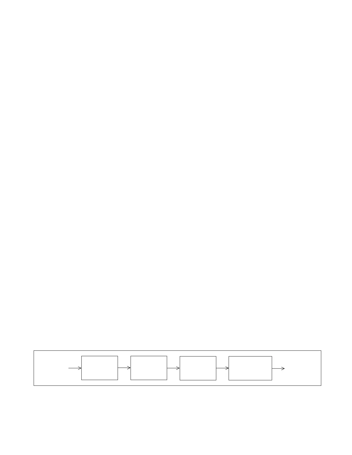
Refer to the block diagram (Figure 11-2) and the schematic diagram (Figure 11-5) for the following
discussion.
The RFL 9780 RF Interface module contains attenuator and amplifier circuitry followed by a
programmable fourth order band-pass filter, which is used to remove excess energy at the receiver
input. The filter consists of two resonant sections, and is adjustable from 30KHz to 535KHz using four
DIP switches. The variable resistors (R16, R20, R46, and R49) are preset at the factory and should not
require any adjustments. Improper setting of these variable resistors will greatly modify the filter
characteristics. The DIP switches are set to the desired center frequency using the “Filter Switch
Settings” chart (Table 11-2). A “0” means that the switch is “OFF” and a “1” means that the switch is
“ON”. Switch position 1 of each DIP switch is the most significant value, while switch position 10 is
the least significant value. The filter maintains a relatively flat bandwidth of approximately 10 kHz
independent of center frequency.
The input signal at pin A28 is first attenuated by 0 to 50 dB in 10 dB steps, as selected by J2. Diodes
CR5 and CR6 provide high voltage transient protection. The signal is then amplified by U4 and U5.
The gain of the first amplifier (U4) is either 4 or 40, depending on the selection of J3. The gain of
amplifier U5 is variable between 0.1 and 5.1, as determined by the setting of the GAIN potentiometer
R16. The output of this amplifier (TP3) drives the programmable band-pass filter.
The band-pass filter consists of two cascaded state-variable filter sections. Each section consists of
three operational amplifiers, two configured as integrators and one as an inverter. Changing the time
constants of the integrators controls the resonant frequency. This is accomplished by switching in
various resistor values using S1 through S4. R15 and R45 control the Q of the sections.
Potentiometers R16 and R46 adjust for small phase errors in the circuits, which can drastically effect
the performance at the higher frequencies of operation. R20 and R49 adjust the frequency of the high
and low frequency sections, respectively. Jumper J1 allows the same signal to drive both sections in
parallel for calibration. Normally, the band-pass output of the low frequency section is used to drive the
high-pass section, and the low-pass output of this section is taken as the entire filter output. The low-
pass output of the second state-variable filter section is used to provide a more arithmetically
symmetrical filter response for the complete band-pass filter.
An analog switch is used to gate the filter output to the output pin (A15) on the board. Switch U9 uses a
series-shunt switch configuration to control this output, where one switch is closed when the other is
open. A third switch section is used to create an inverted control signal. The control signal is generated
from a Schmitt trigger circuit formed by Q2 and Q3. Transistor Q1 is used as an emitter follower to
reduce the current drain on the timing circuits formed by C13, R53 and CR3. Zener diode CR4 provides
an 8.2 volt offset between the timing circuit and the level comparator circuit. The circuit squelches the
output of the filter for about 0.5 seconds at power up to eliminate possible relatively large transient
output voltages at startup.
Figure 11-2. RF Interface Module block diagram
INPUT
ATTENUATOR
BUFFER
MPLIFIER
MPLIFIER
PROGRAMMABLE
FILTER
TO
IF/BF
MODULE
FROM
I/O
MODULE
 Loading...