Saia-Burgess Controls AG
Manual I/O-modules for PCD1 │ PCD2 series │ Document 27-600 – Release ENG09 │ 2019-05-01
5-46
I/O modules PCD1|PCD2
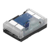
PCD2.B100
5
General technical data on inputs and outputs
Resistance to interference:
acc. to IEC 801-4
4 kV under direct coupling
2 kV under capacitive coupling (whole trunk group)
Internal current consumption:
(from +5 V bus)
1 … 25mA
typically 15 mA
Internal current consumption:
(from V+ bus)
0 mA
External current consumption: Load current
Terminals: Pluggable 10-pole screw terminal block
(4 405 4847 0), for wires up to 1.5 mm²
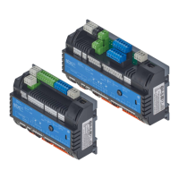
LEDs and connection terminals
Input filter
Recovery diodes
LEDs
Screw terminals
9 8 7 6 5 4 3 2 1 0
Bus connector
Bus interface
Output transistors (MOSFET)
The module contains 8 LEDs:
● 2LEDsaredirectlytriggeredbythepureinputs.
● 2LEDsaredirectlytriggeredbythepureoutputs.
● 4LEDsaretriggeredbytheinputsofthecombinedinputs/outputsandtherefore
always indicate voltage status at the I/O terminal.
If the combined I/Os are used as outputs, the following should be noted:
TheLEDsofcombinedoutputsE/A2 … E/A5onlylightupwhentheoutputishigh
and a supply voltage of 24 V is connected.
Mixing the combined inputs/outputs
If combined I/Os are used as inputs in source operation, i.e. with sending devices
which either apply +24 V to the input or are open, the low status of an open input
can be overwritten as high if the corresponding output at the same address is set
in error. However, if the input is shifted to 0 V with a changeover contact and the
corresponding output is set in error, the MOS-FET can be destroyed, as it is not
short circuit protected. For this reason, only positive-switching contacts should be
used.