Lesson 1 – Analog Modules
68
30M AWG
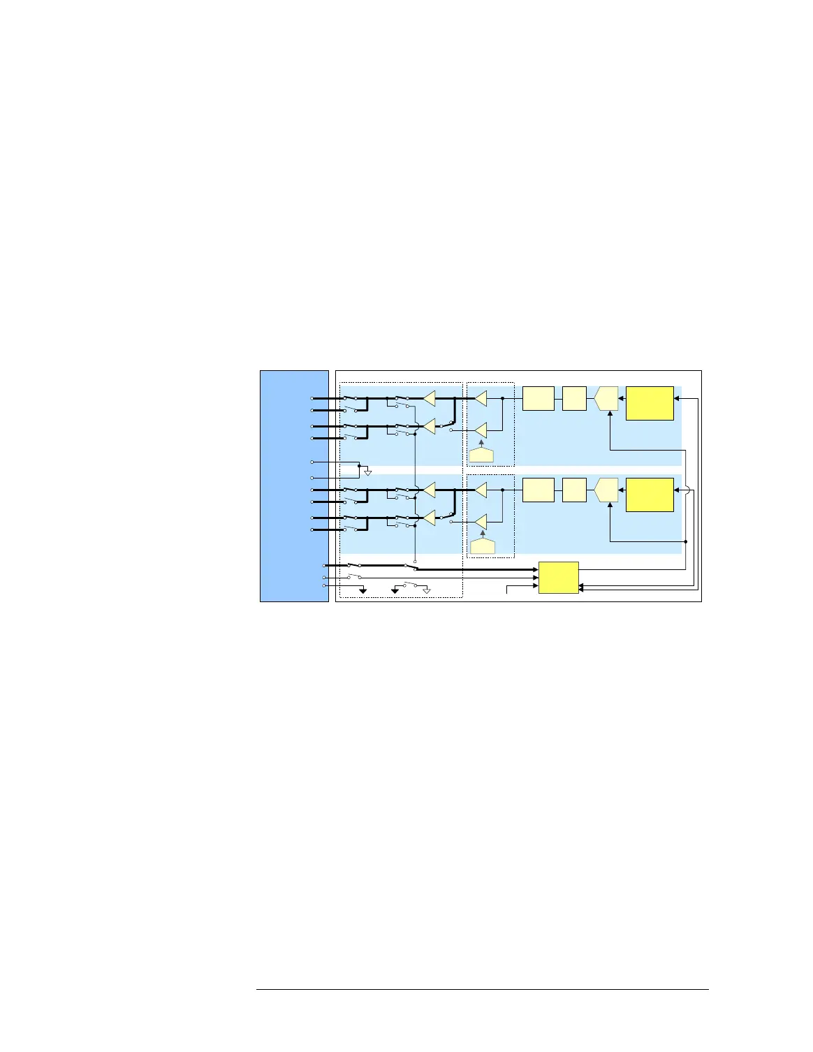
The following figure shows the block diagram of the 30M AWG
(WGE); the bold lines show the single-ended output routes of the
WGE.
The WGE is a single-slot analog module installed in the testhead,
and has two identical AWGs that share the trigger/timing system.
As shown in the following figure, the SYNC CLK pin (which is the
trigger input pin) and the timing generator are shared between its
two AWGs.
Each AWG (called an AWG core) has the own waveform memory
and sequencer. Thus, the two AWG cores can generate different
waveforms and generate them with different waveform sequences.
Block Diagram of WGE (Single-ended Output Routes)
Both the AWG cores can be used simultaneously in multi-site
testing, cross-talk signal generation, IQ baseband signal generation,
or test application where the two signals are generated with the
common sampling rate and common trigger signal. You can differ
the start timing of the two AWG cores slightly by setting the trigger
delay parameter (max. 10 ns difference) plus the initial discard
parameter (max. 1023 sampling periods difference).
The single-ended signal and differential signal can be generated
from the pins shown in the following table.
Pogo Pin
DAC
Output Multiplexer
A+ (16/Mode1)
D+ (10/Mode4)
C+ (12/Mode3)
B+ (14/Mode2)
DGND
Non-inverse
Non-inverse
Inverse
Master Clock
Output Amp
CCLK Stop / Sequencer Start
SYNC CLK (04)
SYNC DATA (03)
Timing
Generator
Offset DAC
Inverse
C– (11/Mode7)
D– (09/Mode8)
A– (15/Mode5)
B– (13/Mode6)
AGND
Conversion Clock (CCLK)
Offset DAC
DAC
Filter
Attenu-
ator
Filter
Attenu-
ator
Sequencer/
Waveform
Memory
AGND
(GND for SYNC CLK)
Sequencer/
Waveform
Memory
Core 1
Core 2
 Loading...