287
8331B–AVR–03/12
Atmel AVR XMEGA AU
22. SPI – Serial Peripheral Interface
22.1 Features
• Full-duplex, three-wire synchronous data transfer
• Master or slave operation
• Lsb first or msb first data transfer
• Eight programmable bit rates
• Interrupt flag at the end of transmission
• Write collision flag to indicate data collision
• Wake up from idle sleep mode
• Double speed master mode
22.2 Overview
The Serial Peripheral Interface (SPI) is a high-speed synchronous data transfer interface using
three or four pins. It allows fast communication between an XMEGA device and peripheral
devices or between several microcontrollers. The SPI supports full-duplex communication.
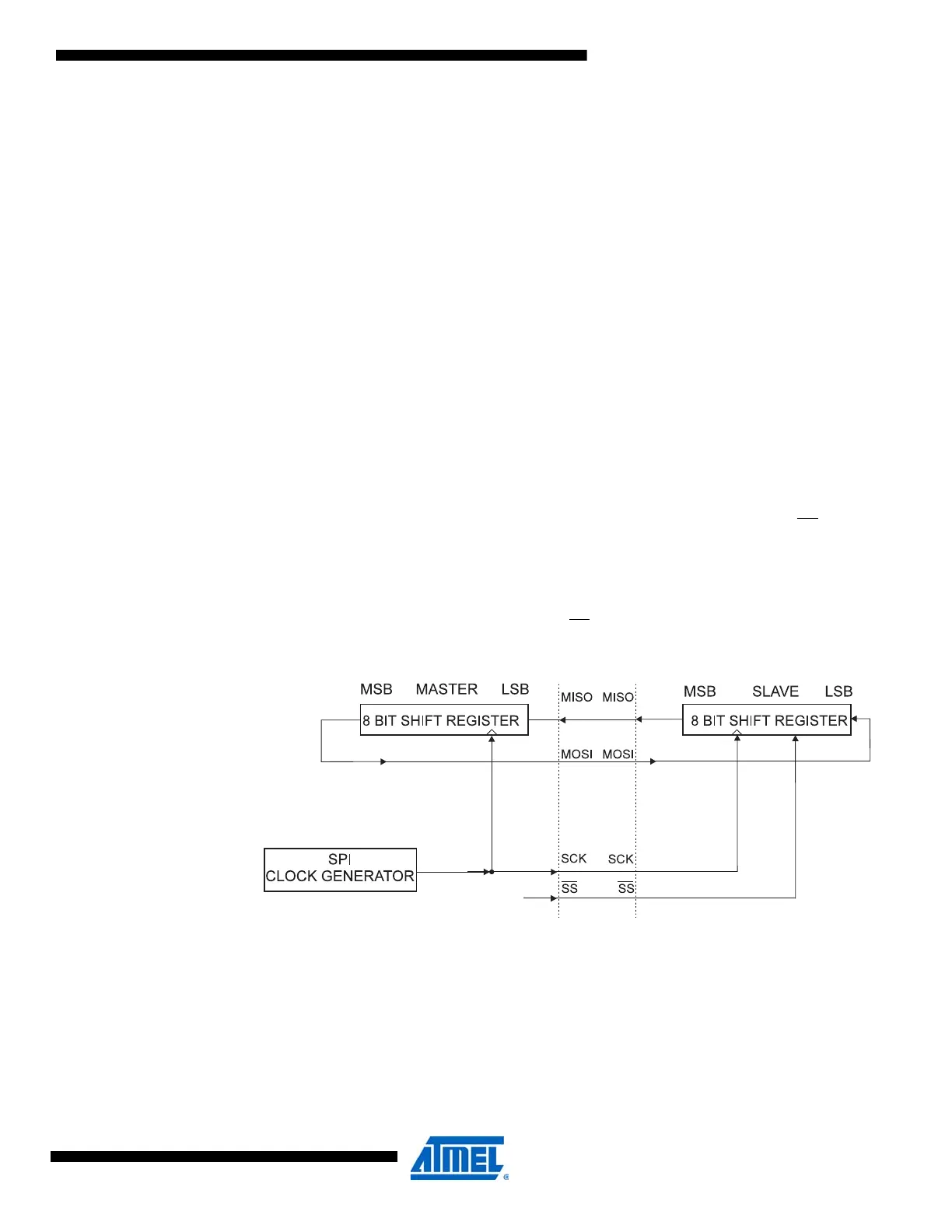
A device connected to the bus must act as a master or slave.The master initiates and controls all
data transactions. The interconnection between master and slave devices with SPI is shown in
Figure 22-1 on page 287. The system consists of two shift registers and a master clock genera-
tor. The SPI master initiates the communication cycle by pulling the slave select (SS
) signal low
for the desired slave. Master and slave prepare the data to be sent in their respective shift regis-
ters, and the master generates the required clock pulses on the SCK line to interchange data.
Data are always shifted from master to slave on the master output, slave input (MOSI) line, and
from slave to master on the master input, slave output (MISO) line. After each data packet, the
master can synchronize the slave by pulling the SS
line high.
Figure 22-1. SPI master-slave interconnection.
The SPI module is unbuffered in the transmit direction and single buffered in the receive direc-
tion. This means that bytes to be transmitted cannot be written to the SPI DATA register before
the entire shift cycle is completed. When receiving data, a received character must be read from
the DATA register before the next character has been completely shifted in. Otherwise, the first
byte will be lost.
In SPI slave mode, the control logic will sample the incoming signal on the SCK pin. To ensure
correct sampling of this clock signal, the minimum low and high periods must each be longer
than two CPU clock cycles.
SHIFT
ENABLE

 Loading...


