289
8331B–AVR–03/12
Atmel AVR XMEGA AU
22.5 Data Modes
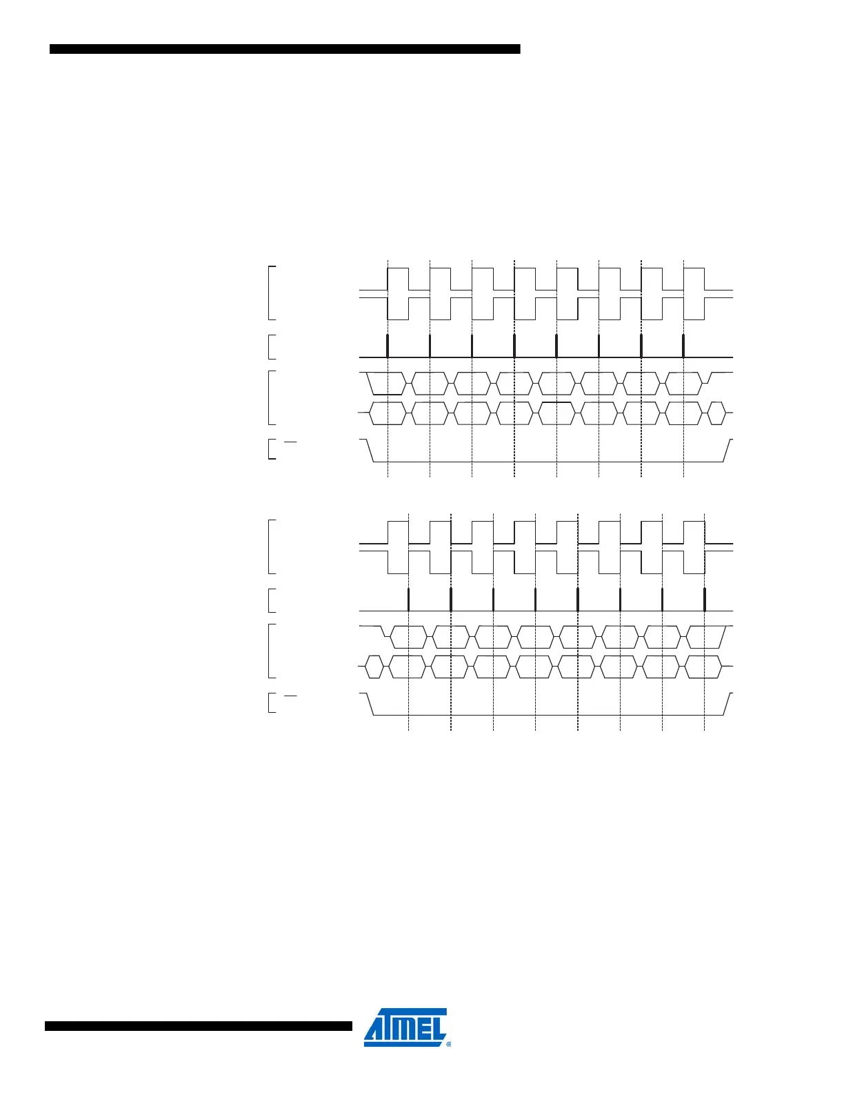
There are four combinations of SCK phase and polarity with respect to serial data. The SPI data
transfer formats are shown in Figure 22-2. Data bits are shifted out and latched in on opposite
edges of the SCK signal, ensuring sufficient time for data signals to stabilize.
The leading edge is the first clock edge of a clock cycle. The trailing edge is the last clock edge
of a clock cycle.
Figure 22-2. SPI transfer modes.
22.6 DMA Support
DMA support on the SPI module is available only in slave mode. The SPI slave can trigger a
DMA transfer as one byte has been shifted into the DATA register. It is possible, however, to use
the XMEGA USART in SPI mode and then have DMA support in master mode. For details, refer
to ”USART in Master SPI Mode” on page 307.
Bit 1
Bit 6
LSB
MSB
Mode 0
SAMPLE I
MOSI/MISO
CHANGE 0
MOSI PIN
CHANGE 0
MISO PIN
Mode 2
SS
MSB
LSB
Bit 6
Bit 1
Bit 5
Bit 2
Bit 4
Bit 3
Bit 3
Bit 4
Bit 2
Bit 5
MSB first (DORD = 0)
LSB first (DORD = 1)
Mode 1
SAMPLE I
MOSI/MISO
CHANGE 0
MOSI PIN
CHANGE 0
MISO PIN
Mode 3
SS
MSB
LSB
Bit 6
Bit 1
Bit 5
Bit 2
Bit 4
Bit 3
Bit 3
Bit 4
Bit 2
Bit 5
Bit 1
Bit 6
LSB
MSB
MSB first (DORD = 0)
LSB first (DORD = 1)

 Loading...


