199
8331B–AVR–03/12
Atmel AVR XMEGA AU
15.10 Register Description
15.10.1 CTRLA – Control register A
• Bit 7:4 – Reserved
These bits are unused and reserved for future use. For compatibility with future devices, always
write these bits to zero when this register is written.
• Bit 3:0 – CLKSEL[3:0]: Clock Select
These bits select clock source for the timer/counter according to Table 15-2 on page 199. The
clock select is identical for both high- and low-byte timer/counters.
15.10.2 CTRLB – Control register B
• Bit 7:0 – HCMPENx/LCMPENx: High/Low Byte Compare Enable x
Setting these bits will enable the compare output and override the port output register for the
corresponding OCn output pin.
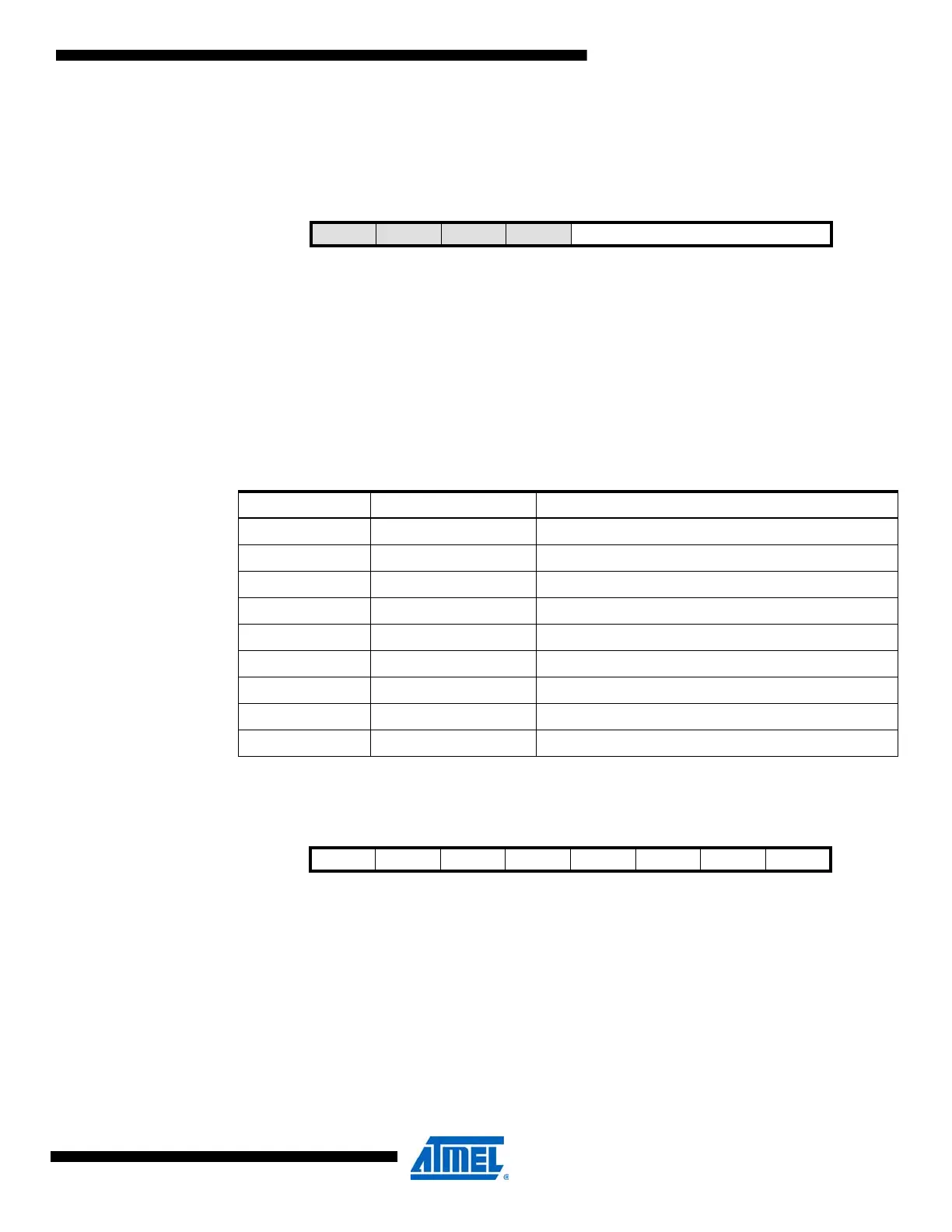
Bit 76543210
+0x00 – – – – CLKSEL[3:0] CTRLA
Read/Write R R R R R/W R/W R/W R/W
Initial Value00000000
Table 15-2. Clock Select
CLKSEL[3:0] Group Configuration Description
0000 OFF None (i.e., timer/counter in OFF state)
0001 DIV1 Prescaler: Clk
PER
0010 DIV2 Prescaler: Clk
PER
/2
0011 DIV4 Prescaler: Clk
PER
/4
0100 DIV8 Prescaler: Clk
PER
/8
0101 DIV64 Prescaler: Clk
PER
/64
0110 DIV256 Prescaler: Clk
PER
/256
0111 DIV1024 Prescaler: Clk
PER
/1024
1nnn EVCHn Event channel n, n= [0,...,7]
Bit 76543210
+0x01 HCMPEND HCMPENC HCMPENB HCMPENA LCMPEND LCMPENC LCMPENB LCMPENA CTRLB
Read/Write R/W R/W R/W R/W R/W R/W R/W R/W
Initial Value 0 0 0 0 0 0 0 0

 Loading...


