370
8331B–AVR–03/12
Atmel AVR XMEGA AU
28.16 Register Description – ADC
28.16.1 CTRLA – Control register A
• Bit 7:6 – DMASEL[1:0]: DMA Request Selection
To allow one DMA channel to serve more than one ADC channel, the DMA request from the
channels can be combined into a common DMA request. See Table 28-1 for details.
• Bit 5:2 – CHSTART[3:0]: Channel Start Single Conversion
Setting any of these bits will start a conversion on the corresponding ADC channel. Setting sev-
eral bits at the same time will start conversions on all selected ADC channels, starting with the
channel with the lowest number. These bits are cleared by hardware when the conversion has
started.
• Bit 1 – FLUSH: Pipeline Flush:
Setting this bit will flush the ADC pipeline. When this is done, the ADC clock is restarted on the
next peripheral clock edge, and all conversions in progress are aborted and lost.
After the flush and the ADC clock restart, the ADC will resume where it left off; i.e., if a channel
sweep was in progress or any conversions were pending, these will enter the ADC pipeline and
complete.
• Bit 0 – ENABLE: Enable
Setting this bit enables the ADC.
28.16.2 CTRLB – ADC Control register B
• Bit 7 – IMPMODE: Gain Stage Impedance Mode
This bit controls the impedance mode of the gain stage. See GAIN setting with ADC channel
register description for more information.
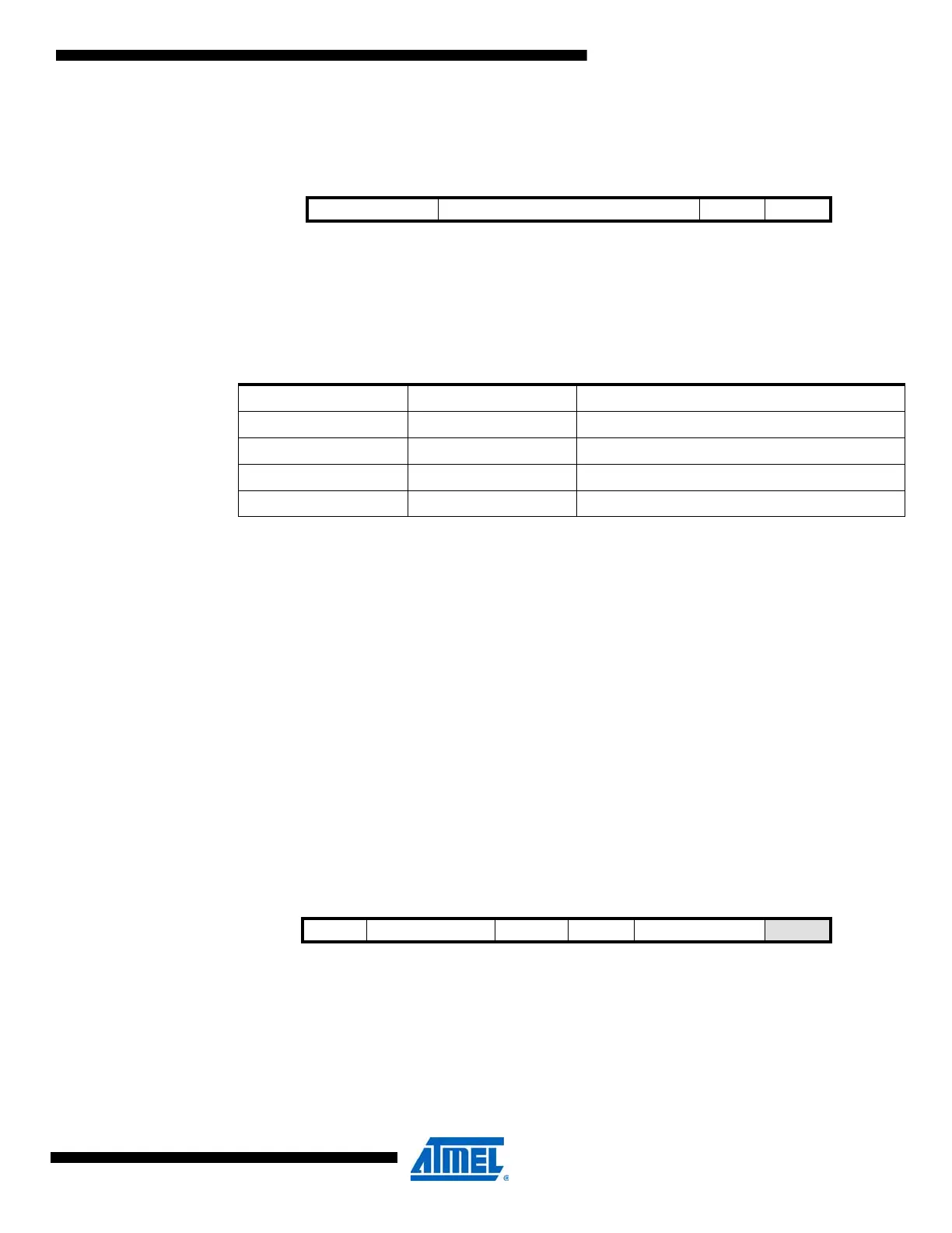
Bit 76543210
+0x00 DMASEL[1:0] CHSTART[3:0] FLUSH ENABLE CTRLA
Read/Write R/W R/W R/W R/W R/W R/W R/W R/W
Initial Value 0 0 0 0 0 0 0 0
Table 28-1. DMA request selection.
DMASEL[1:0] Group Configuration Description
00 OFF No combined DMA request
01 CH01 Common request for ADC channels 0 and 1
10 CH012 Common request for ADC channels 0, 1, and 2
11 CH0123 Common request for ADC channels 0, 1, 2, and 3
Bit 765 4 3 2 1 0
+0x01 IMPMODE CURRLIMIT[1:0] CONVMODE FREERUN RESOLUTION[1:0] –CTRLB
Read/Write R/W R/W R/W R/W R/W R/W R/W R
Initial Value 0 0 0 0 0 0 0 0

 Loading...


