413
8331B–AVR–03/12
Atmel AVR XMEGA AU
31.5.2 Scanning the PDI Pins
Two observe-only cells are inserted to make the combined RESET and PDI_CLK pin and the
PDI_DATA pin observable. Even though the PDI_DATA pin is bidirectional, it is only made
observable in order to avoid any extra logic on the PDI_DATA output path.
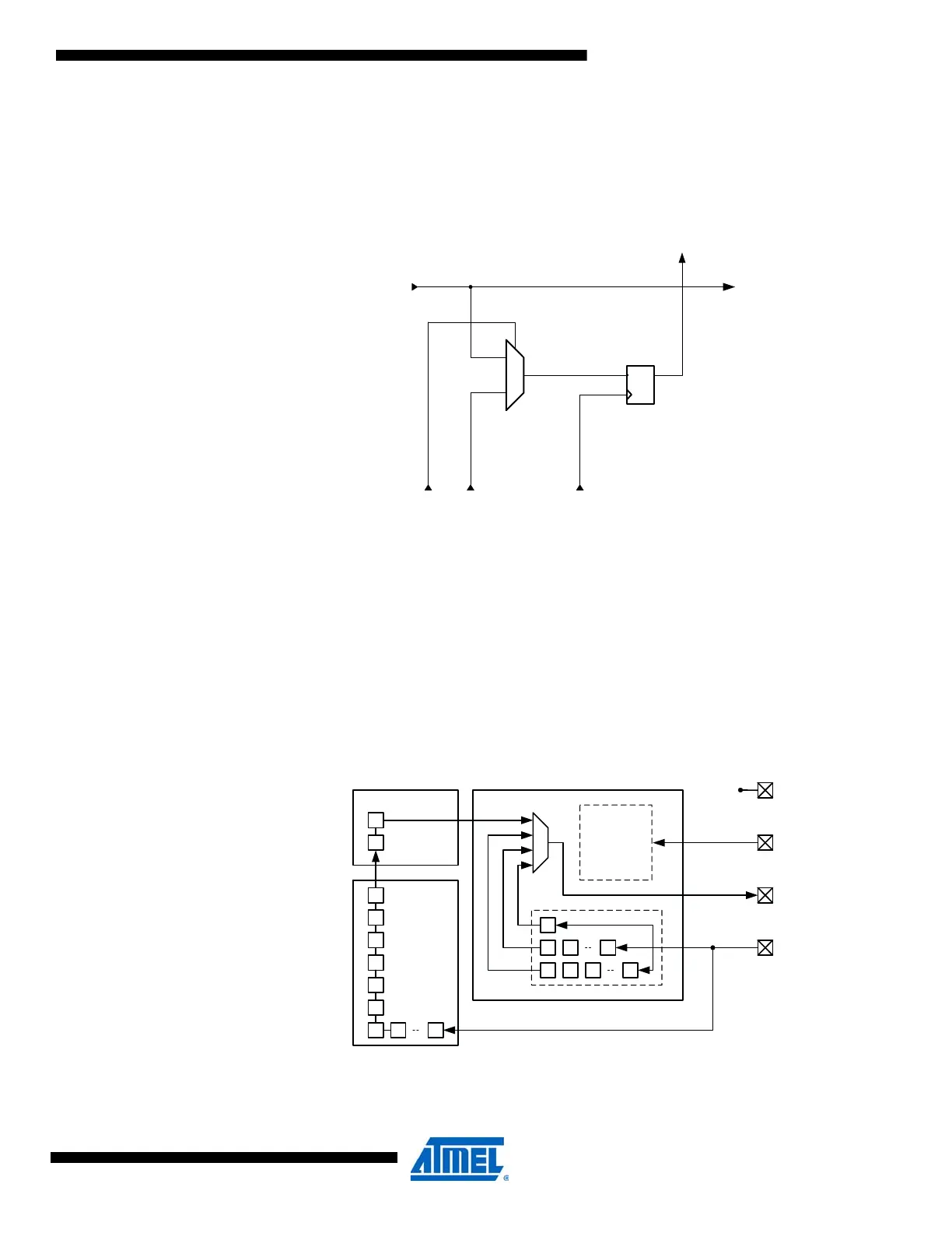
Figure 31-3. An observe-only input cell.
31.6 Data Registers
The supported data registers that can be connected between TDI and TDO are:
• Bypass register (Ref: register A in Figure 31-4 on page 413).
• Device identification register (Ref: register C in Figure 31-4 on page 413).
• Boundary scan chain (Ref: register D in Figure 31-4 on page 413).
• PDICOM data register (Ref: register B in Figure 31-4 on page 413)
Figure 31-4. JTAG data register overview.
D
Q
From last
cell
Clock DR
To next cell
To system
logic
From system
pin
Shift DR
1
0
D
D
TDI
A
B B B
C C C C
TDO
TMS
D
D
D
D
D
D
D
D D
I/O PORTS
PDI JTAG
TCK
to all TCK
registers
Internal registers
JTAG Boundary-scan chain
TAP
CTRL

 Loading...


