367
8331B–AVR–03/12
Atmel AVR XMEGA AU
done and available, and so on. In this mode, up to eight conversions are ongoing at the same
time.
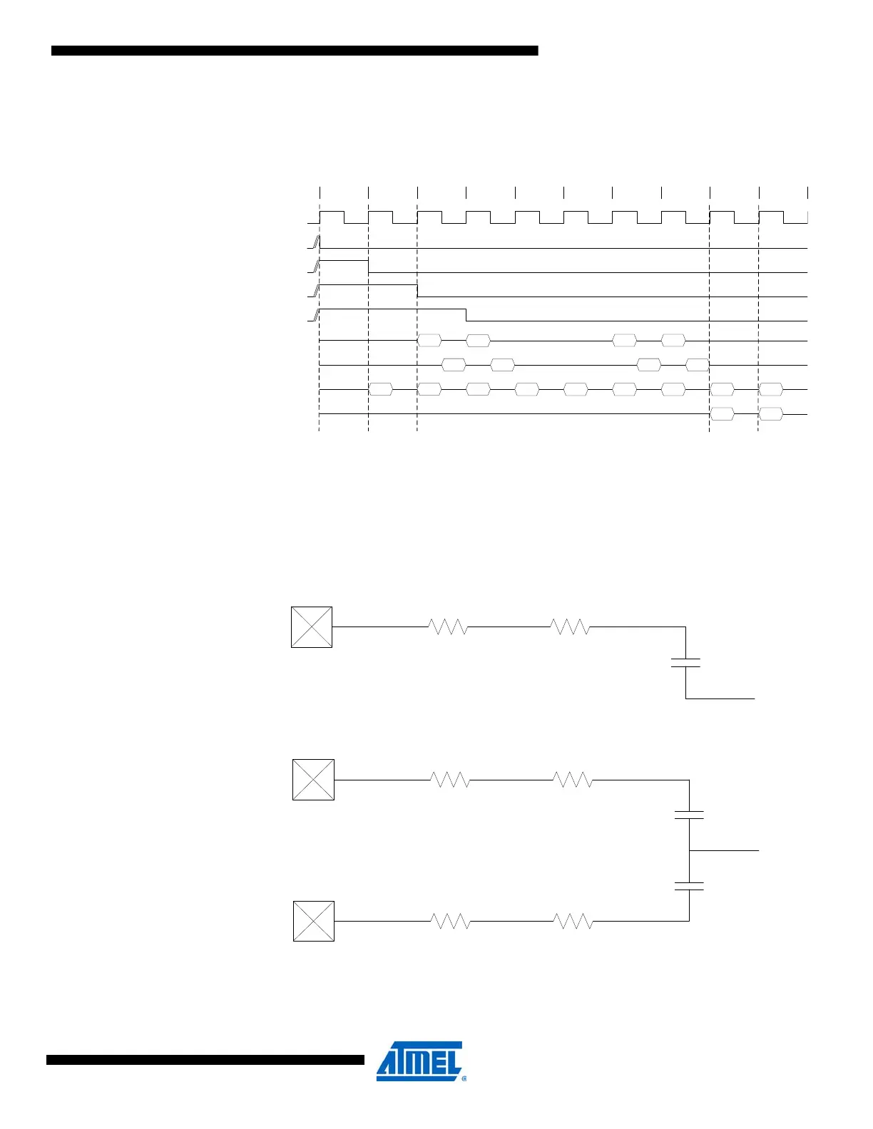
Figure 28-18. ADC timing for free running mode.
28.10 ADC Input Model
The voltage input must charge the sample and hold (S/H) capacitor in the ADC in order to
achieve maximum accuracy. Seen externally, the ADC input consists of an input resistance
(R
in
= R
channel
+ R
switch
) and the S/H capacitor (C
sample
). Figure 28-19 on page 367 and Figure 28-
20 on page 367 show the ADC input channels.
Figure 28-19. ADC input for single-ended measurements.
Figure 28-20. ADC input for differential measurements and differential measurements with gain.
START CH1, wo/GAIN
ADC SAMPLE
START CH0, wo/GAIN
GAINSTAGE SAMPLE
GAINSTAGE AMPLIFY
START CH1, w/GAIN
START CH0, w/GAIN
CONV COMPLETE
0
1
CLK
ADC
12345678
9 10
2
3
2
3
2 3
2
3
0
1 2
3 0 1 2 3 0
R
channel
R
switch
C
Sample
VCC/2
Positive
input
R
channel
R
switch
C
Sample
VCC/2
Positive
input
R
channel
R
switch
C
Sample
Negative
input

 Loading...


