182
8331B–AVR–03/12
Atmel AVR XMEGA AU
14.12 Register Description
14.12.1 CTRLA – Control register A
• Bit 7:4 – Reserved
These bits are unused and reserved for future use. For compatibility with future devices, always
write these bits to zero when this register is written.
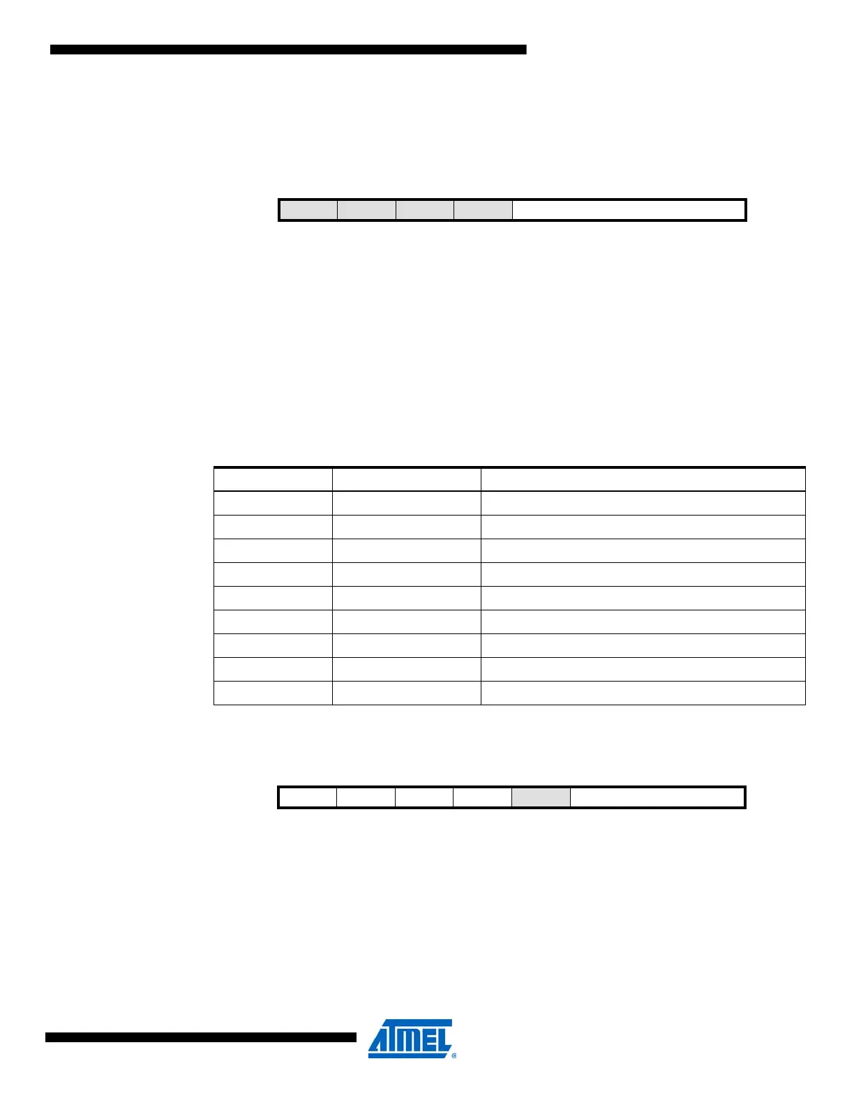
• Bit 3:0 – CLKSEL[3:0]: Clock Select
These bits select the clock source for the timer/counter according to Table 14-3.
CLKSEL=0001 must be set to ensure a correct output from the waveform generator when the hi-
res extension is enabled.
14.12.2 CTRLB – Control register B
• Bit 7:4 – CCxEN: Compare or Capture Enable
Setting these bits in the FRQ or PWM waveform generation mode of operation will override the
port output register for the corresponding OCn output pin.
When input capture operation is selected, the CCxEN bits enable the capture operation for the
corresponding CC channel.
Bit 76543210
+0x00 – – – – CLKSEL[3:0] CTRLA
Read/Write R R R R R/W R/W R/W R/W
Initial Value00000000
Table 14-3. Clock select options.
CLKSEL[3:0] Group Configuration Description
0000 OFF None (i.e, timer/counter in OFF state)
0001 DIV1 Prescaler: Clk
0010 DIV2 Prescaler: Clk/2
0011 DIV4 Prescaler: Clk/4
0100 DIV8 Prescaler: Clk/8
0101 DIV64 Prescaler: Clk/64
0110 DIV256 Prescaler: Clk/256
0111 DIV1024 Prescaler: Clk/1024
1nnn EVCHn Event channel n, n= [0,...,7]
Bit 76543210
+0x01 CCDEN CCCEN CCBEN CCAEN – WGMODE[2:0] CTRLB
Read/Write R/W R/W R/W R/W R R/W R/W R/W
Initial Value 0 0 0 0 0 0 0 0
 Loading...


