453
8331B–AVR–03/12
Atmel AVR XMEGA AU
34. Peripheral Module Address Map
The address maps show the base address for each peripheral and module in XMEGA. All
peripherals and modules are not present in all XMEGA devices, refer to device data sheet for
the peripherals module address map for a specific device.
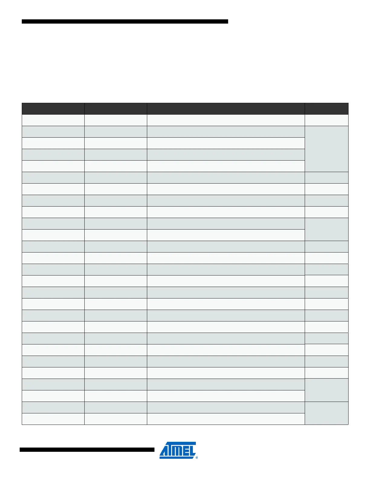
Table 34-1. Peripheral module address map.
Base address Name Description Page
0x0000 GPIO General purpose IO registers 52
0x0010 VPORT0 Virtual Port 0
162
0x0014 VPORT1 Virtual Port 1
0x0018 VPORT2 Virtual Port 2
0x001C VPORT3 Virtual Port 2
0x0030 CPU CPU 18
0x0040 CLK Clock control 103
0x0048 SLEEP Sleep controller 110
0x0050 OSC Oscillator control 103
0x0060 DFLLRC32M DFLL for the 32 MHz internal RC oscillator
103
0x0068 DFLLRC2M DFLL for the 2 MHz RC oscillator
0x0070 PR Power reduction 110
0x0078 RST Reset controller 118
0x0080 WDT Watch-dog timer 133
0x0090 MCU MCU control 52
0x00A0 PMIC Programmable multilevel interrupt controller 142
0x00B0 PORTCFG Port configuration 162
0x00C0 AES AES module 327
0x00D0 CRC CRC module 327
0x00F0 VBAT Battery backup system 127
0x0100 DMA DMA controller 58
0x0180 EVSYS Event system 81
0x01C0 NVM Non volatile memory (NVM) controller 50
0x0200 ADCA Analog to digital converter on port A
381
0x0200 ADCB Analog to digital converter on port B
0x0300 DACA Digital to analog converter on port A
392
0x0320 DACB Digital to analog converter on port B

 Loading...


