147
8331B–AVR–03/12
Atmel AVR XMEGA AU
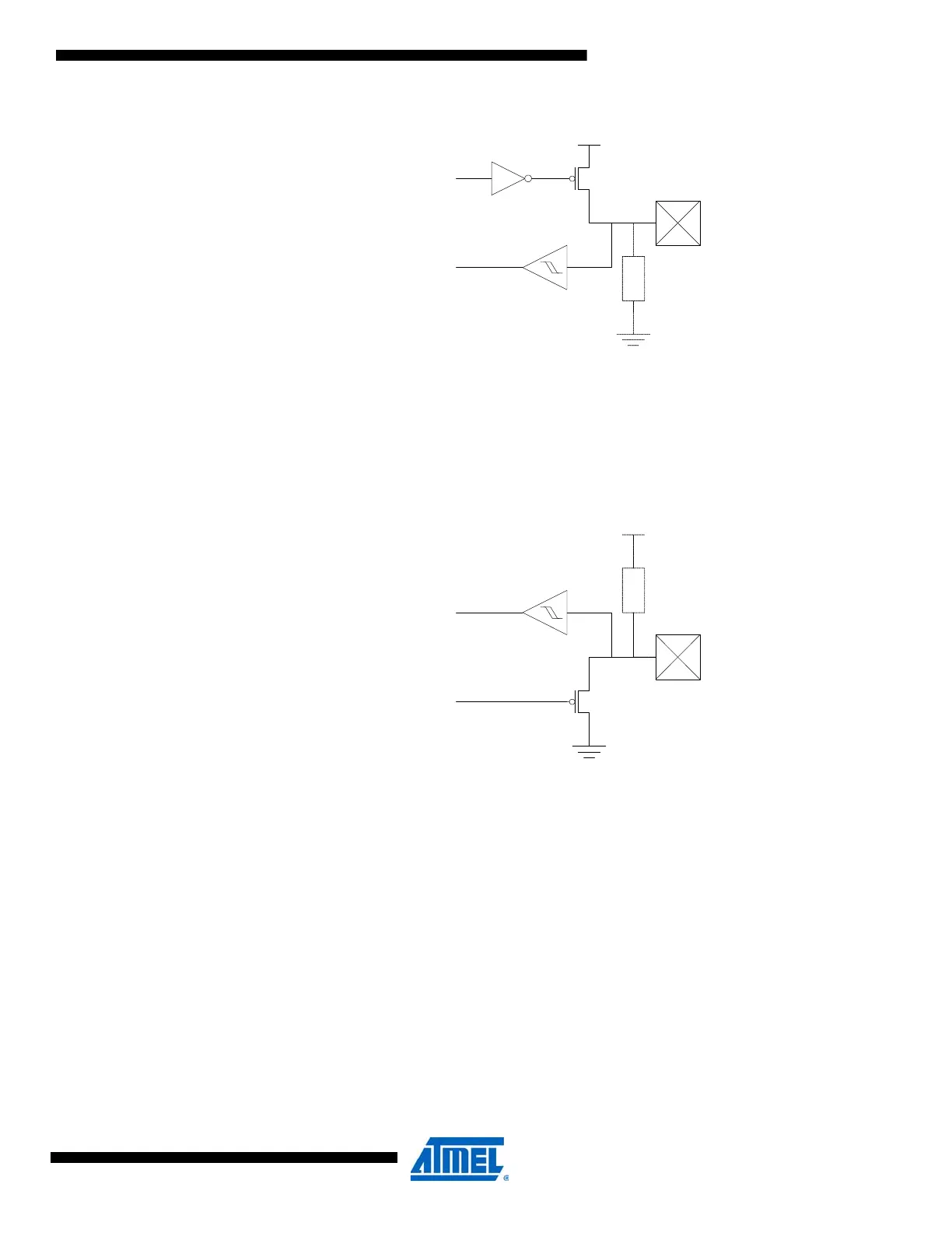
Figure 13-6. Output configuration - Wired-OR with optional pull-down.
13.3.4 Wired-AND
In the wired-AND configuration, the pin will be driven low when the corresponding bits in the
OUT and DIR registers are written to zero. When the OUT register is set to one, the pin is
released allowing the pin to be pulled high with the internal or an external pull-resistor. If internal
pull-up is used, this is also active if the pin is set as input.
Figure 13-7. Output configuration - Wired-AND with optional pull-up.
13.4 Reading the Pin Value
Independent of the pin data direction, the pin value can be read from the IN register, as shown in
Figure 13-1 on page 144. If the digital input is disabled, the pin value cannot be read. The IN
register bit and the preceding flip-flop constitute a synchronizer. The synchronizer introduces a
delay on the internal signal line. Figure 13-8 on page 148 shows a timing diagram of the syn-
chronization when reading an externally applied pin value. The maximum and minimum
propagation delays are denoted as t
pd,max
and t
pd,min
, respectively.

 Loading...


