340
8331B–AVR–03/12
Atmel AVR XMEGA AU
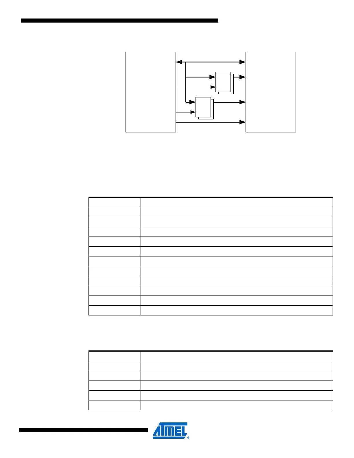
Figure 27-8. Multiplexed SRAM LPC connection using ALE1 and ALE2.
27.7 SDRAM Configuration
Chip Select 3 on the EBI can be configured from SDRAM operation, and the EBI must be config-
ured as a three-port or four-port interface. The SDRAM can be configured for 4-bit or 8-bit data
bus, and four-Port interface must be used for 8-bit data bus. The SDRAM interface signals from
the EBI to the SDRAM is listed in Table 27-2 on page 340.
27.7.1 Supported Commands
The SDRAM commands that are supported by the EBI is listed in Table 27-3 on page 340.
EBI SRAM
A[15:8]/
AD[7:0]
ALE1
ALE2
D
Q
G
D
Q
G
D[7:0]
A[7:0]
A[15:8]
A[19:16]A[19:16]
Table 27-2. SDRAM Interface signals.
Signal Description
CS Chip select
WE Write enable
RAS Row address strobe
CAS Column address strobe
DQM Data mask signal/ output enable
CKE Clock enable
CLK Clock
BA[1:0] Bank address
A[12:0] Address bus
A[10] Precharge
D[7:0] Data bus
Table 27-3. Supported SDRAM commands.
Command Description
NOP No Operation
ACTIVE Activate the selected bank and select the row
READ Input the starting column address and begin the burst read operation
WRITE Input the starting column address and begin the burst write operation
PRECHARGE Deactivate the open row of selected bank or all banks

 Loading...


