292
8331B–AVR–03/12
Atmel AVR XMEGA AU
• Bit 6 – WRCOL: Write Collision Flag
The WRCOL flag is set if the DATA register is written during a data transfer. This flag is cleared
by first reading the STATUS register when WRCOL is set, and then accessing the DATA
register.
• Bit 5:0 – Reserved
These bits are unused and reserved for future use. For compatibility with future devices, always
write these bits to zero when this register is written.
22.7.4 DATA – Data register
The DATA register is used for sending and receiving data. Writing to the register initiates the
data transmission, and the byte written to the register will be shifted out on the SPI output line.
Reading the register causes the shift register receive buffer to be read, returning the last byte
successfully received.
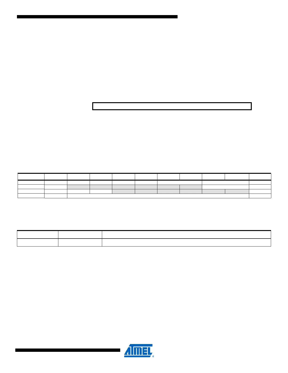
22.8 Register Summary
22.9 Interrupt vector Summary
Bit 76543210
+0x03 DATA[7:0] DATA
Read/Write R/W R/W R/W R/W R/W R/W R/W R/W
Initial Value00000000
Address Name Bit 7 Bit 6 Bit 5 Bit 4 Bit 3 Bit 2 Bit 1 Bit 0 Page
+0x00 CTRL CLK2X ENABLE DORD MASTER MODE[1:0] PRESCALER[1:0] 290
+0x01 INTCTRL – – – – – – INTLVL[1:0] 291
+0x02 STATUS IF WRCOL – – – – – –291
+0x03 DATA DATA[7:0] 292
Table 22-4. SPI interrupt vector and its offset word address.
Offset Source Interrupt Description
0x00 SPI_vect SPI interrupt vector

 Loading...


