37
8331B–AVR–03/12
Atmel AVR XMEGA AU
bits is possible by executing a chip erase command. All other access; using the TIF and OCD, is
blocked if any of the Lock Bits are written to 0. These bits do not block any software access to
the memory.
Note: 1. Program the Fuse Bits and Boot Lock Bits before programming the Lock Bits.
4.17 Register Description – Production Signature Row
4.17.1 RCOSC2M – Internal 2MHz Oscillator Calibration register
• Bit 7:0 – RCOSC2M[7:0]: Internal 2MHz Oscillator Calibration Value
This byte contains the oscillator calibration value for the internal 2MHz oscillator. Calibration of
the oscillator is performed during production test of the device. During reset this value is auto-
matically loaded into calibration register B for the 2MHz DFLL. Refer to ”CALB – DFLL
Calibration register B” on page 102 for more details.
4.17.2 RCOSC2MA – Internal 2MHz Oscillator Calibration register
• Bit 7:0 – RCOSC2MA[7:0]: Internal 2MHz Oscillator Calibration Value
This byte contains the oscillator calibration value for the internal 2MHz oscillator. Calibration of
the oscillator is performed during production test of the device. During reset this value is auto-
matically loaded into calibration register A for the 2MHz DFLL. Refer to ”CALA – DFLL
Calibration Register A” on page 101 for more details.
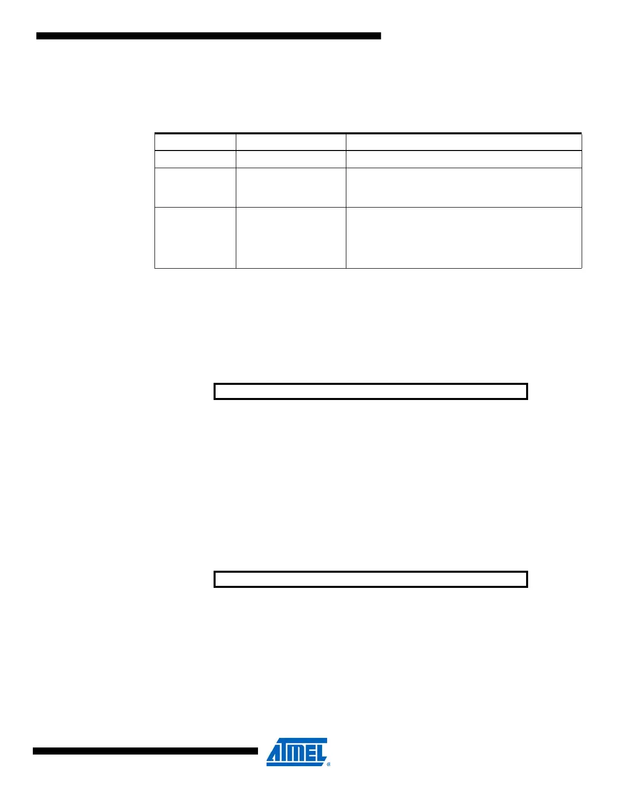
Table 4-12. Lock bit protection mode.
LB[1:0] Group Configuration Description
11 NOLOCK3 No lock – no memory locks enabled.
10 WLOCK
Write lock – programming of the flash and EEPROM is
disabled for the programming interface. Fuse bits are
locked for write from the programming interface.
00 RWLOCK
Read and write lock – programming and
read/verification of the flash and EEPROM are disabled
for the programming interface. The lock bits and fuses
are locked for read and write from the programming
interface.
Bit 7654 3 2 1 0
+0x00 RCOSC2M[7:0] RCOSC2M
Read/Write R R R R R R R R
Initial Value x x x x x x x x
Bit 7654 3 2 1 0
+0x01 RCOSC2MA[7:0] RCOSC2MA
Read/Write R R R R R R R R
Initial Value x x x x x x x x

 Loading...


