NXP Semiconductors
UM11227
NTM88 family of tire pressure monitor sensors
UM11227 All information provided in this document is subject to legal disclaimers. © NXP B.V. 2020. All rights reserved.
User manual Rev. 6 — 24 April 2020
131 / 205
• Internal multiplexer capable of converting 14 signals including two external pins, and
internal VREFL or VREFH
• Clock select control options (ADICLK)
– bus clock
– bus clock divided by 2
– external source (ALTCLK) – either on-chip or off-chip, as defined by chip-level
hookup
– internal generated source (ADACK) asynchronous to the bus clock
• Conversion executed asynchronous to bus clock
– Conversion can be performed while operating at any bus clock frequency (>0 Hz to
20 MHz)
• Clock rate control options (ADIV) – selected clock, divided by 1, 2, 4, or 8.
• Triggerable through software or external hardware (ADTRG)
– for external hardware, trigger is either on-chip or off-chip, as defined by chip-level
hookup
• Auto-compare function (ACFE)
– digital comparator configurable for either "greater than or equal" or "less
than" (ACFGT)
– no conversion complete (COCO) flag setting and no data transfer on false compare
• Runs in stop mode (when ADICLK selects internal asynchronous clock source)
– capable of asynchronous stop wake-up
– continuous compare does not wake system until a true compare conversion
• Analog temperature sensor
– used via conversion on one of the selectable internal channels
• Configurable conversion reference source (REFSEL) – currently an unadvertised
feature
– Normal V
REFH
/V
REFL
pad source (the default source – REFSEL[1:0] = 0 0)
– V
DDA
/V
SSA
pad source
– Alternate source (i.e., on-chip band gap reference circuit)
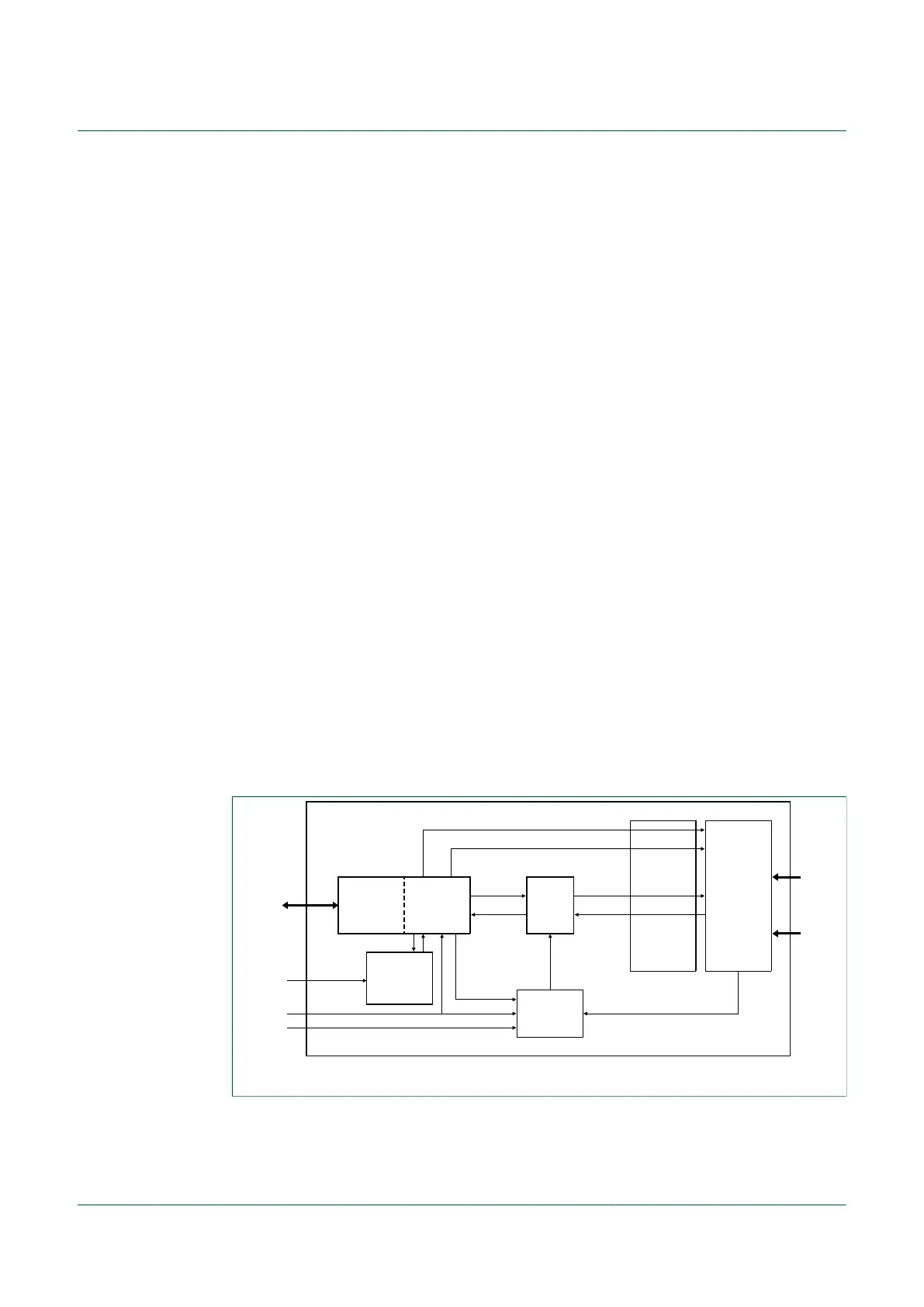
aaa-031059
BUS
INTERFACE
IP interface
signals
IP BUS
REGISTERS
HARDWARE
TRIGGER
DETECT
SAR
ADCLK
SELECT
control
ADTRG
ALTTRG
ALTCLK
bus clock
status, data
control
ADCH, ADLPC, asclk_en
reference select control (3)
ADC
SCAN
WRAPPER
ANALOG
HARD
BLOCK
VDDAD,
VSSAD,
VREFH (3),
VREFL (3)
4 on-chip +
24 off-chip
AD channels
data
ADACLK
ADCLK
ADIV, ADICLK
Figure 40. Analog to digital converter block diagram

 Loading...