NXP Semiconductors
UM11227
NTM88 family of tire pressure monitor sensors
UM11227 All information provided in this document is subject to legal disclaimers. © NXP B.V. 2020. All rights reserved.
User manual Rev. 6 — 24 April 2020
170 / 205
10.24.2 FMC program and erase times
Before any program or erase command can be accepted, the FLASH clock divider
register (FCDIV) must be written to set the internal clock for the FLASH module to a
frequency (f
FCLK
) between 150 kHz and 200 kHz. This register can be written only once,
so normally this write is performed during reset initialization. FCDIV cannot be written if
the access error flag, FACCERR in FSTAT, is set. The user must ensure that FACCERR
is not set before writing to the FCDIV register. One period of the resulting clock (1/f
FCLK
)
is used by the command processor to time program and erase pulses. An integer number
of these timing pulses are used by the command processor to complete a program or
erase command.
Table 183 shows program and erase times. The bus clock frequency, and FCDIV
determine the frequency of FCLK (f
FCLK
). The time for one cycle of FCLK is t
FCLK
= 1/
f
FCLK
. The times are shown as a number of cycles of FCLK and as an absolute time for
the case where t
FCLK
= 5 us. Program and erase times shown include overhead for the
command state machine and enabling and disabling of program and erase voltages.
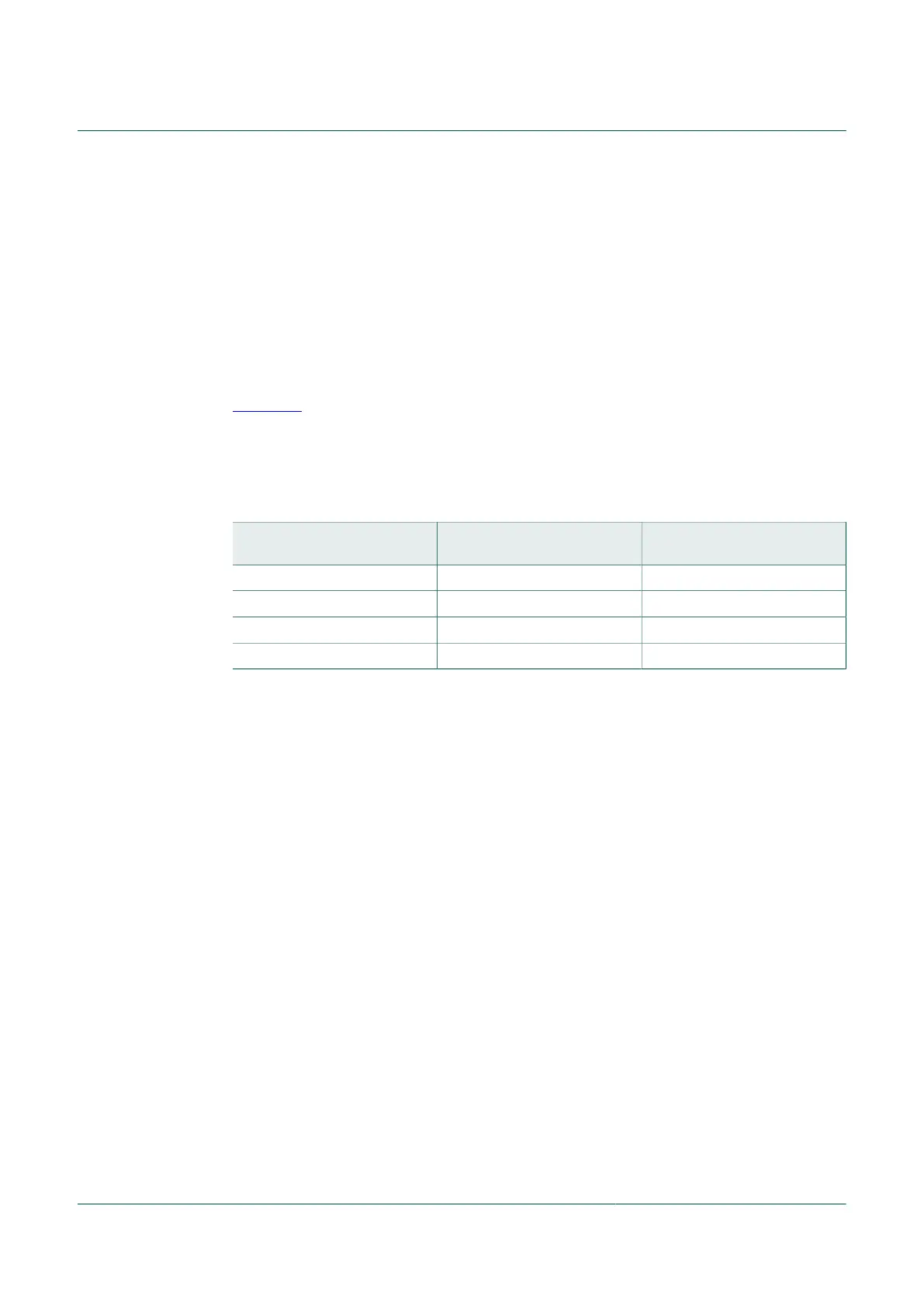
Table 183. Program and erase times
Parameter Cycles of FCLK Time
[1]
assuming FCLK = 200
kHz
Byte program 9 45 µs
Byte program (burst) 4 20 µs
Page erase 4000 20 ms
Mass erase 20,000 100 ms
[1] Burst program time excludes start/end overhead.
10.24.3 FMC program and erase command execution
The steps for executing any of the commands are listed below. The FCDIV register must
be initialized and any error flags cleared before beginning command execution. The
command execution steps are:
1. Write a data value to an address in the FLASH array. The address and data
information from this write is latched into the FLASH interface. This write is a required
first step in any command sequence. For erase and blank check commands, the
value of the data is not important. For page erase commands, the address may be
any address in the 512-byte page of FLASH to be erased. For mass erase and blank
check commands, the address can be any address in the FLASH memory. Whole
pages of 512 bytes are the smallest block of FLASH that may be erased. Do not
program any byte in the FLASH more than once after a successful erase operation.
Reprogramming bits to a byte which is already programmed is not allowed without
first erasing the page in which the byte resides or mass erasing the entire FLASH
memory. Programming without first erasing may disturb data stored in the FLASH.
2. Write the command code for the desired command to FCMD. The five valid
commands are blank check ($05), byte program ($20), burst program ($25), page
erase ($40), and mass erase ($41). The command code is latched into the command
buffer.
3. Write a 1 to the FCBEF bit in FSTAT to clear FCBEF and launch the command
(including its address and data information).

 Loading...