NXP Semiconductors
UM11227
NTM88 family of tire pressure monitor sensors
UM11227 All information provided in this document is subject to legal disclaimers. © NXP B.V. 2020. All rights reserved.
User manual Rev. 6 — 24 April 2020
138 / 205
aaa- 031060
SS_B
SPIEN
SCLK
/16
MOSI MISO
Input Shift Register Output Shift Register
Input Latch Register
R = Read Address Decode
W = Write Address Decode
W = stuff bits W = Write Data
R/W Decode
RST*
Clock
R/W
spi_bus_req
spi_bus_grant
spi_reset_b
Data
Address
R/W Echo
Parity Decode
W = Write Address Echo
W = Status Encode W = Write Data Echo
R = Status Encode R = Read Data
Parity Encode
Slave SPI State Machine
Output Latch Register
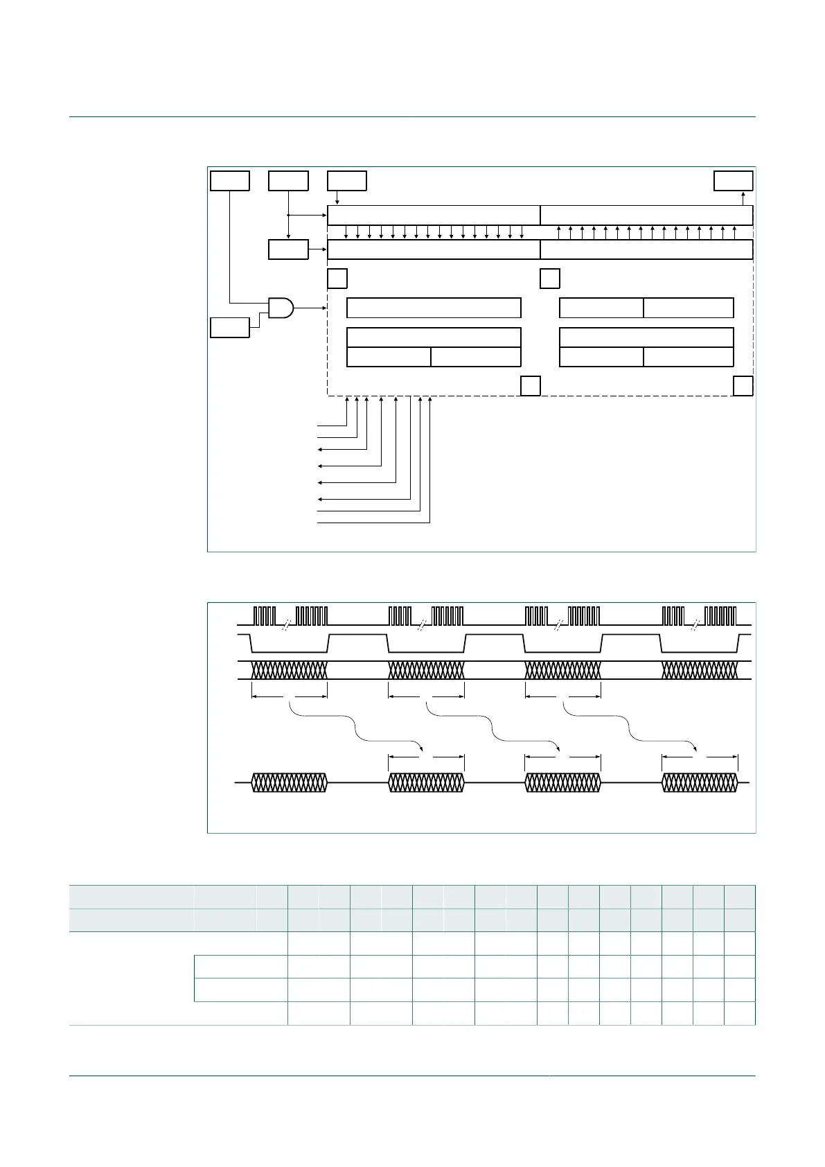
Figure 41. Slave SPI state machine
Transaction event schedule; T1 being the first master transmission, R1 being the first
slave response being concurrent with T2 being the second master transmission:
aaa- 031061
T1 T2
R1 R2 R3
T3
MISO
MOSI
SS_B
SCLK
Figure 42. SPI message response protocol
10.18.1 SPI protocol definition
Clock cycle c1 c2 c3 c4 c5 c6 c7 c8 c9 c10 c11 c12 c13 c14 c15 c16
Bit assignment b15 b14 b13 b12 b11 b10 b9 b8 b7 b6 b5 b4 b3 b2 b1 b0
T1 0 a12 a11 a10 a9 a8 a7 a6 a5 a4 a3 a2 a1 a0 p1 p0
R0 r s4 s3 s2 s1 s0 r r r r r r r r p1 p0
T2 t t t t t t t t t t t t t t p1 p0
Read byte from
Address
R1 0 s4 s3 s2 s1 s0 d7 d6 d5 d4 d3 d2 d1 d0 p1 p0

 Loading...