250
8331B–AVR–03/12
Atmel AVR XMEGA AU
20.13.4 ADDR – Address register
• Bit 7 – Reserved
This bit is unused and reserved for future use. For compatibility with future devices, always write
this bit to zero when this register is written.
• Bit 6:0 – ADDR[6:0]: Device Address
These bits contain the USB address the device will respond to.
20.13.5 FIFOWP – FIFO Write Pointer register
• Bit 7:5 – Reserved
These bits are unused and reserved for future use. For compatibility with future devices, always
write these bits to zero when this register is written.
• Bit 4:0 – FIFOWP[4:0]: FIFO Write Pointer
These bits contain the transaction complete FIFO write pointer. This register must be read only
by the CPU or DMA controller. Writing this register will flush the FIFO write and read pointers.
20.13.6 FIFORP – FIFO Read Pointer register
• Bit 7:5 – Reserved
These bits are unused and reserved for future use. For compatibility with future devices, always
write these bits to zero when this register is written.
• Bit 4:0 – FIFORP[4:0]: FIFO Read Pointer
These bits contain the transaction complete FIFO read pointer. This register must only be read
by the CPU or DMA controller. Writing this register will flush the FIFO write and read pointer.
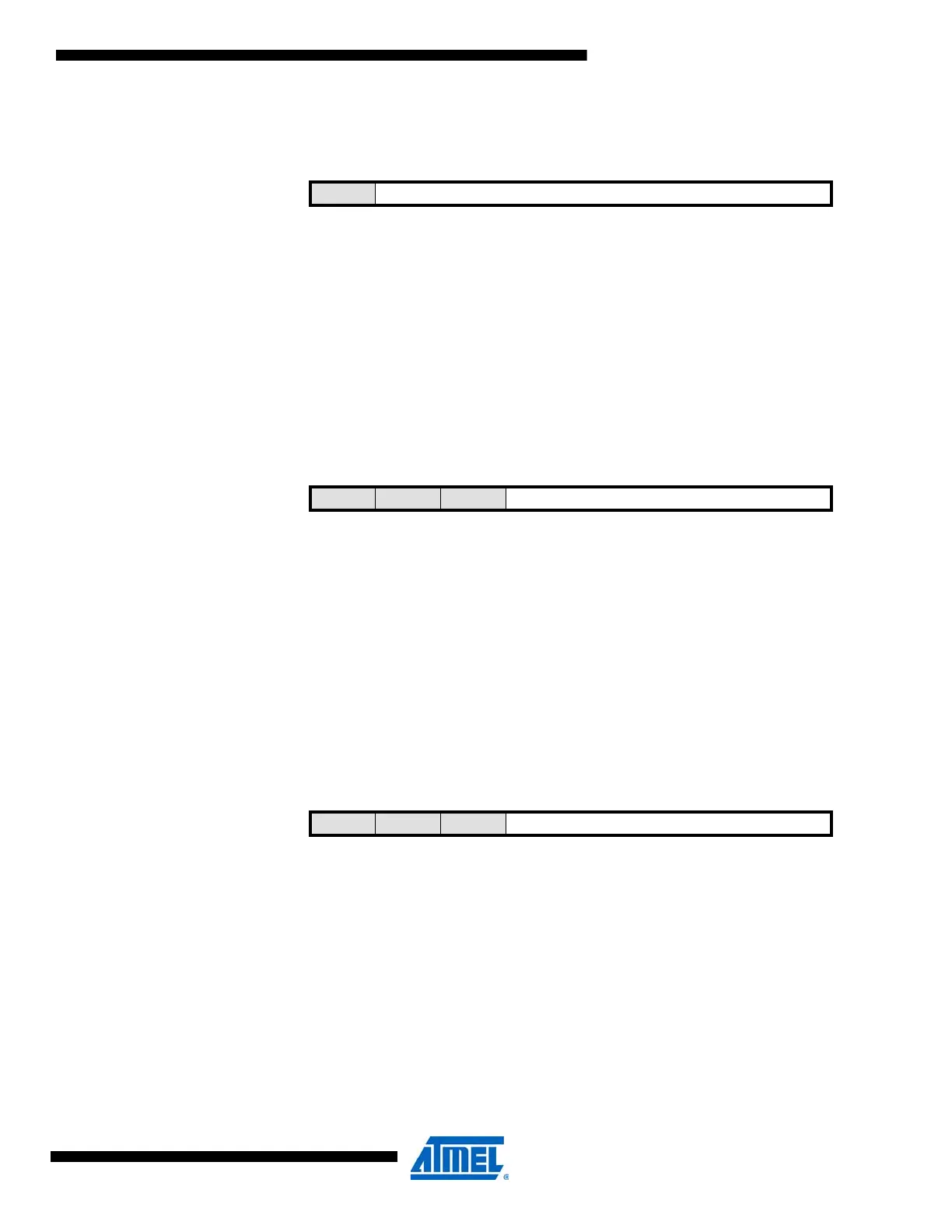
Bit 76543210
+0x03 – ADDR[6:0] ADDR
Read/Write R R/W R/W R/W R/W R/W R/W R/W
Initial Value 0 0 0 0 0 0 0 0
Bit 76543210
+0x04 – –- –- FIFOWP[4:0] FIFOWP
Read/Write R R R R/W R/W R/W R/W R/W
Initial Value 0 0 0 0 0 0 0 0
Bit 76543210
+0x05 – – – FIFORP[4:0] FIFORP
Read/Write R R R R/W R/W R/W R/W R/W
Initial Value 0 0 0 0 0 0 0 0

 Loading...


