353
8331B–AVR–03/12
Atmel AVR XMEGA AU
27.11.2 CTRLB (SRAM) – Control register B
The configuration options for this register depend on the chip select mode configuration. The
register description below is valid when the chip select mode is configured for SRAM or SRAM
LPC.
• Bit 7:3 – Reserved
These bits are unused and reserved for future use.
• Bit 2:0 – SRWS[2:0]: SRAM Wait State
These bits select the number of wait states for SRAM and SRAM LPC access as a number of
Clk
PER2
cycles, according to Table 27-23 on page 353.
27.11.3 CTRLB (SDRAM) – Control register B
The configuration options for this register depend on the chip select mode configuration. The
register description below is valid for CS3 when the chip select mode is configured for SDRAM
.
• Bit 7 – SDINITDONE: SDRAM Initialization Complete
This flag is set at the end of the SDRAM initialization sequence. The flag will remain set as long
as the EBI is enabled and the Chip Select is configured for SDRAM.
• Bit 6:3 – Reserved
These bits are unused and reserved for future use.
• Bit 2 – SDSREN: SDRAM Self-refresh Enable
When this bit is written to one the EBI controller will send a Self-refresh command to the
SDRAM. For leaving the self refresh mode, the bit must be written to zero.
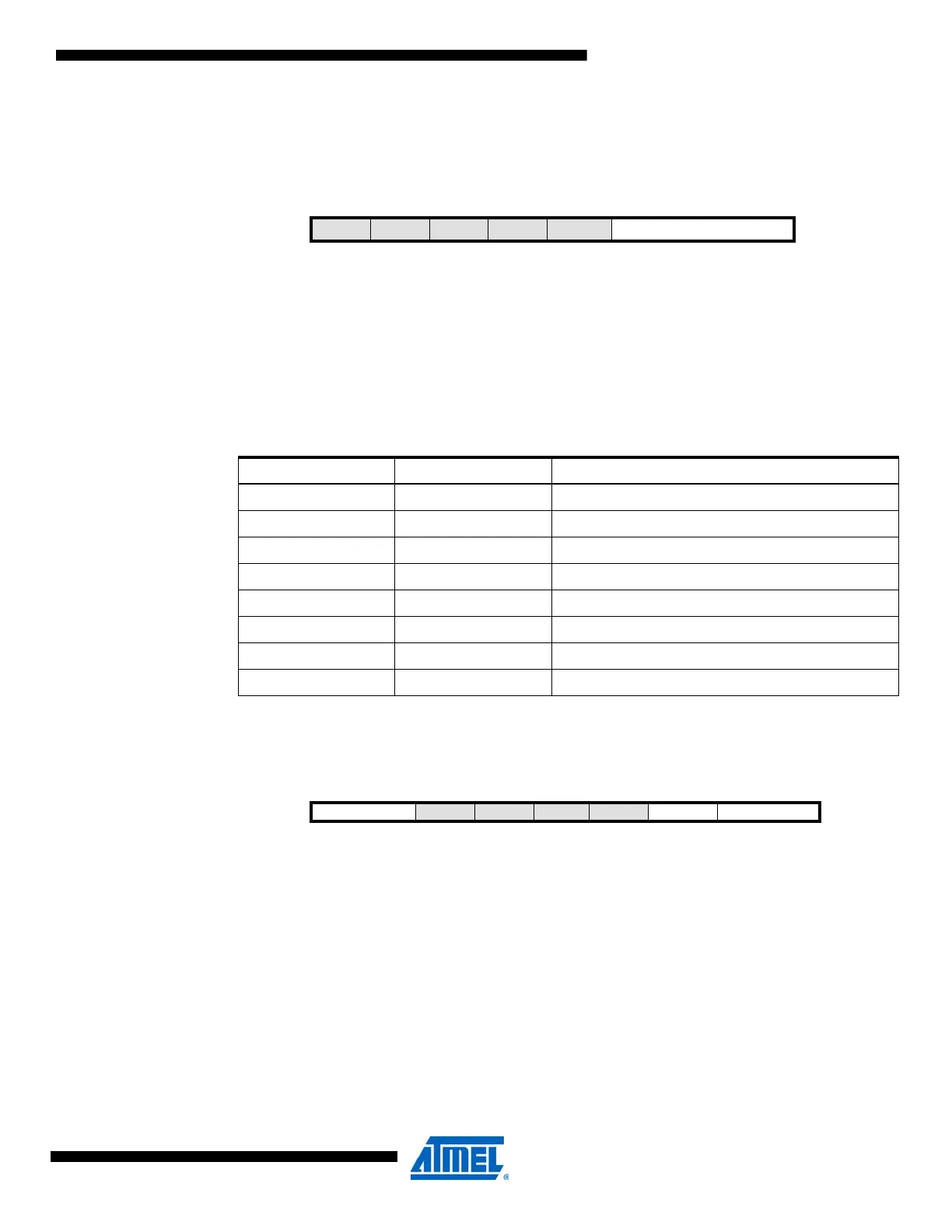
Bit 7654 3 2 10
+0x01
–
– – – –
SRWS[2:0] CTRLB
Read/Write R R R R R R/W R/W R/W
Initial Value0000 0 0 00
Table 27-23. Wait State selection
SRWS[2:0] Group Configuration Description
000 0CLK Zero Clk
PER2
cycles wait state
001 1CLK One Clk
PER2
cycles wait state
010 2CLK Two Clk
PER2
cycles wait state
011 3CLK Three Clk
PER2
cycles wait state
100 4CLK Four Clk
PER2
cycles wait state
101 5CLK Five Clk
PER2
cycles wait state
110 6CLK Six Clk
PER2
cycles wait state
111 7CLK Seven Clk
PER2
cycles wait state
Bit 7 6 5 4 3 2 1 0
+0x01 SDINITDONE
– – – –
SDREN SDMODE[1:0] CTRLB
Read/Write R/W R R R R R/W R/W R/W
Initial Value 0 0 0 0 0 0 0 0

 Loading...


