354
8331B–AVR–03/12
Atmel AVR XMEGA AU
• Bit 1:0 SDMODE[1:0]: SDRAM Mode
These bits select the mode when accessing SDRAM according to Table 27-24 on page 354.
27.11.4 BASEADDR – Base Address register
• Bit 15:4 – BASEADDR[23:12]: Chip Select Base Address
The base address is the lowest address in the address space enabled by a chip select. Together
with the Chip Select Address Size (ASIZE) setting in “CTRLA - Chip Select Control Register A”,
this gives the address space for the Chip Select.
• Bit 3:0 – Reserved
These bits are unused and reserved for future use.
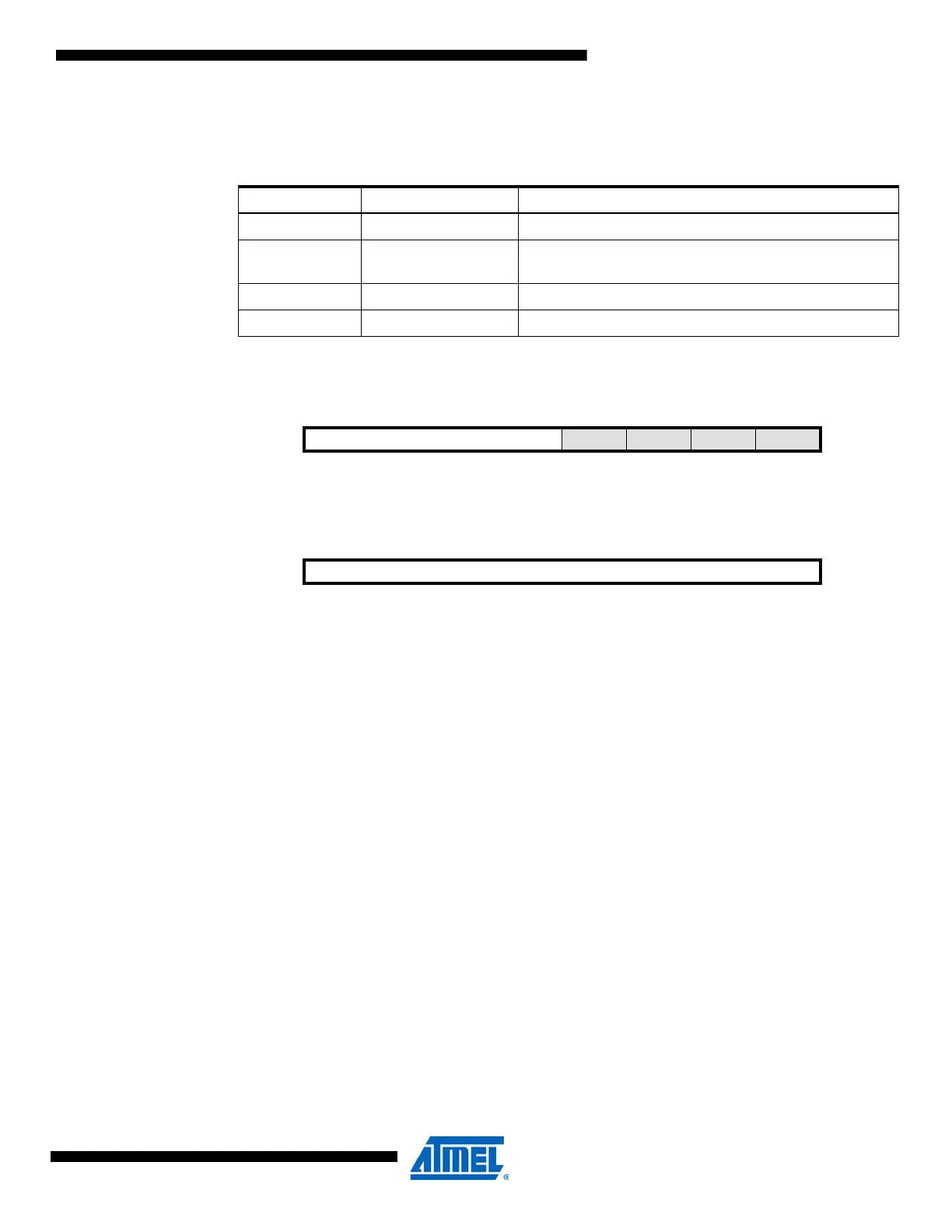
Table 27-24. SDRAM mode
SDMODE[1:0] Group Configuration Description
00 NORMAL Normal mode - access to the SDRAM is decoded normally
01 LOAD
Load Mode - the EBI issues a Load Mode Register
command when the SDRAM is accessed
10 – Reserved
11 – Reserved
Bit 76543210
+0x02 BASEADDR[15:12] – – – – BASEADDRL
Read/Write R/W R/W R/W R/W R R R R
Initial Value
00000000
Bit 76543210
+0x03 BASEADDR[23:16] BASEADDRL
Read/Write R/W R/W R/W R/W R/W R/W R/W R/W
Initial Value
00000000

 Loading...


