422
8331B–AVR–03/12
Atmel AVR XMEGA AU
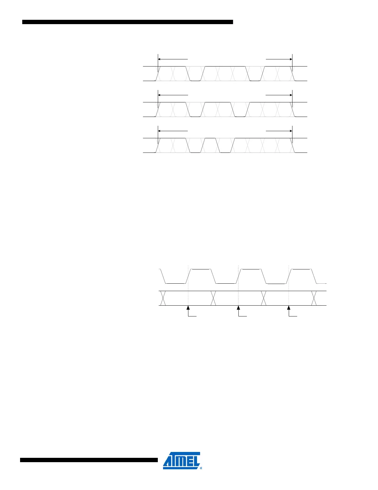
Figure 32-11. Special data characters.
32.4.5 Serial transmission and reception
The JTAG interface supports full-duplex communication. At the same time as input data is
shifted in on the TDI pin, output data is shifted out on the TDO pin. However, PDI communica-
tion relies on half-duplex data transfer. Due to this, the JTAG physical layer operates only in
either transmit (TX) or receive (RX) mode. The available JTAG bit channel is used for control
and status signalling.
The programmer and the JTAG interface operate synchronously on the TCK clock provided by
the programmer. The dependency between the clock edges and data sampling or data change
is fixed. As illustrated in Figure 32-12 on page 422, TDI and TDO is always set up (change) on
the falling edge of TCK, while data always should be sampled on the rising edge of TCK.
Figure 32-12. Changing and sampling data.
32.4.6 Serial Transmission
When data transmission is initiated, a data byte is loaded into the shift register and then out on
TDO. The parity bit is generated and appended to the data byte during transmission. The trans-
mission speed is given by the TCK signal.
If the PDI is in TX mode (as a response to an LD instruction), and a transmission request from
the PDI controller is pending when the TAP controller enters the capture DR state, valid data will
be parallel-loaded into the shift register, and a correct parity bit will be generated and transmitted
along with the data byte in the shift DR state.
If the PDI is in RX mode when the TAP controller enters the capture DR state, an EMPTY byte
will be loaded into the shift register, and the parity bit will be set (forcing a parity error) when data
is shifted out in the shift DR state. This situation occurs during normal PDI command and oper-
and reception.
P1110
1
1101
1 BREAK CHARACTER (BB+P1)
1 DELAY CHARACTER (DB+P1)
1 EMPTY CHARACTER (EB+P1)
P1110
1
1011
P1110
1
0111
TCK
TDI/TDO
SampleSample Sample

 Loading...


