193
Connector Terminals with Transistors Section 5-6
Output Specifications
Note Do not allow the total load current to exceed 2 A and do not allow the load cur-
rent on either the V or G terminal to exceed 1 A.
Components
I/O Indicators
Note m: The first word allocated for the Remote I/O Terminal’s IN Area.
n: The first word allocated for the Remote I/O Terminal’s OUT Area.
Item Specification
Model DRT2-MD32B
DRT2-MD32BV
DRT2-MD32B-1
DRT2-MD32BV-1
Internal I/O common NPN PNP
Output points 16 points
Rated output current 0.3 A/point, 2 A/common (See note.)
Residual voltage 1.2 V max. (at 0.3 A,
between each output termi-
nal and G)
1.2 V max. (at 0.3 A,
between each output termi-
nal and V)
Leakage current 0.1 mA max. 0.1 mA max.
ON delay time 0.5 ms max.
OFF delay time 1.5 ms max.
Number of circuits 16 points with one common circuit
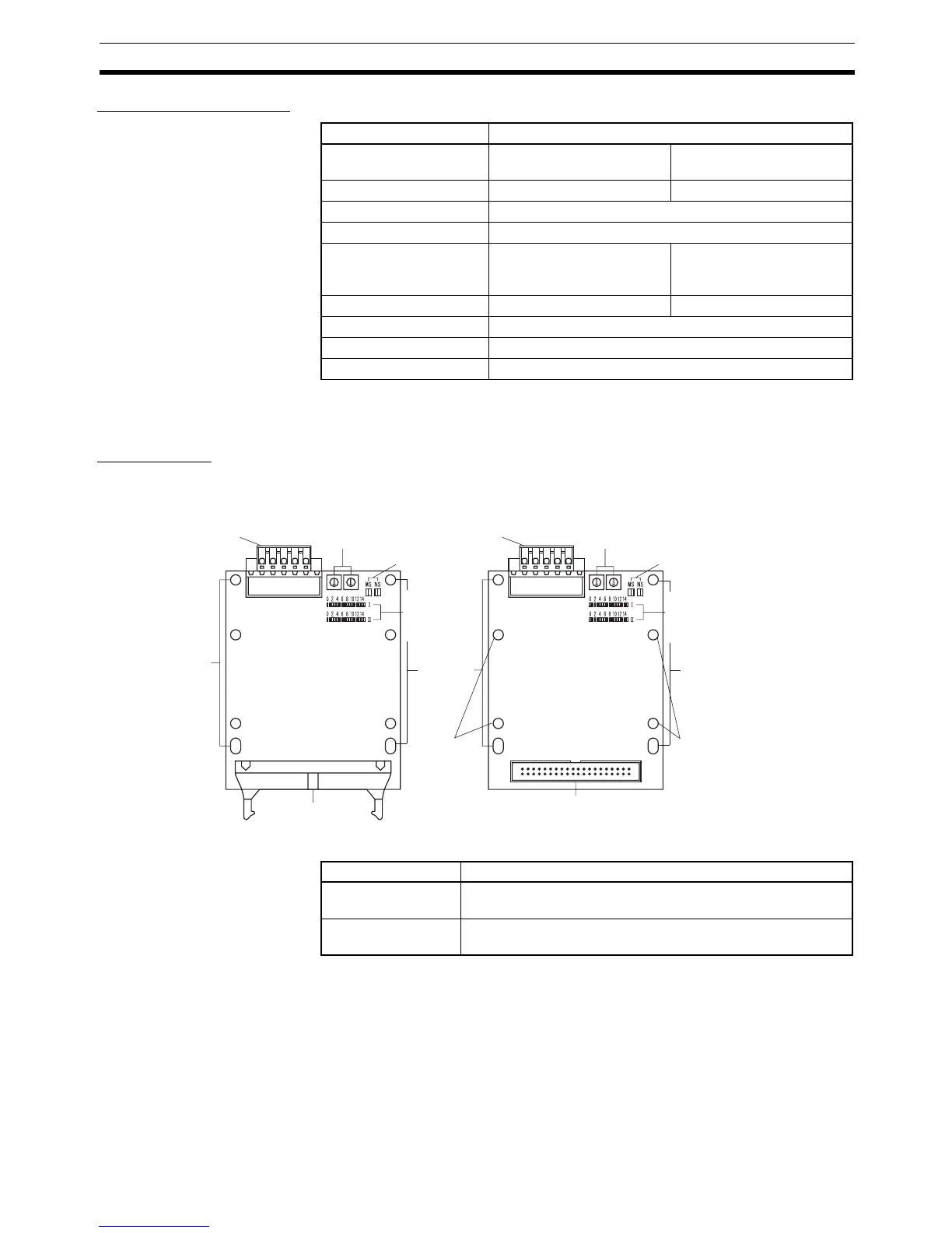
DeviceNet
communications
connector
Node address
switches
(×10)
DeviceNet
operation
indicators
I/O
operation
indicators
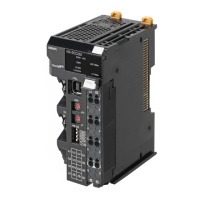
Board
mounting
holes
Board
mounting
holes
I/O connector (MIL) I/O connector
DeviceNet
operation
indicators
Node address
switches
(×10)
DeviceNet
communications
connector
I/O
operation
indicators
Board
mounting
holes
User
customized
board
mounting
holes
User
customized
board
mounting
holes
(×1) (×1)
DRT2-MD32B (NPN)/DRT2-MD32B-1 (PNP)
DRT2-MD32BV (NPN)/DRT2-MD32BV-1 (PNP)
Name Meaning
I0 to I15 Indicate the status of bits (contacts) 0 to 15 in word m. Lit
when input is ON; not lit when input is OFF.
II0 to II15 Indicate the status of bits (contacts) 0 to 15 in word n. Lit when
output is ON; not lit when output is OFF.
 Loading...