Chapter 4 I/O SETTINGS
Chapter 4
I/O Terminal Names and Functions
4-5
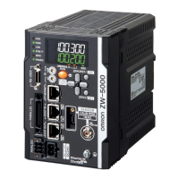
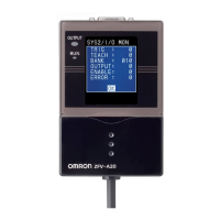
ZW
User’s Manual
Electrical Specifications
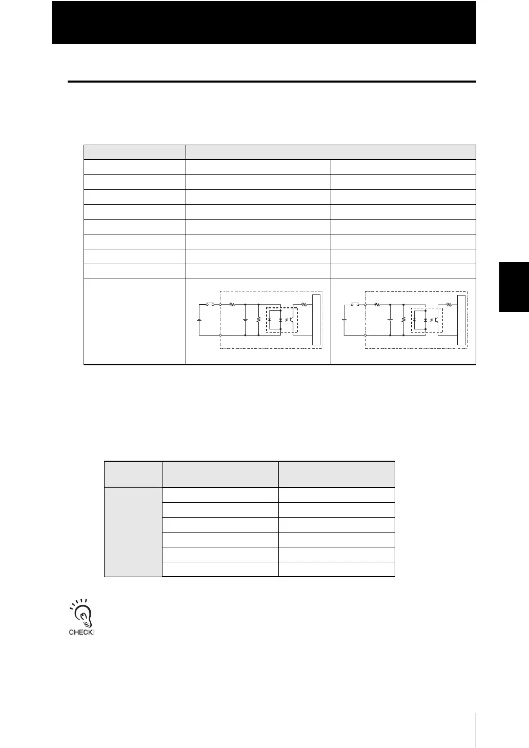
■ Input circuit
*1 ON voltage/ON current
This is the voltage value or current value that makes the signal go OFF to ON.
The ON voltage value becomes the potential difference between COM IN 1/2 and the input terminals.
*2 OFF voltage/OFF current
This is the voltage value or current value that makes the signal go ON to OFF.
The OFF voltage value becomes the potential difference between COM IN 1/2 and the input terminals.
*3 Below is a table giving the COM_IN (input common) and input signal connection correspondence.
Chattering countermeasures
• The sensor is designed with functions to deal with chattering, but if chattering of 100 s or more
occurs, incorrect input due to chattering cannot be prevented. (Input signal changes of less than 100
s are ignored. The input signal is applied when the same level is maintained for 100 s or longer.)
• Always use non-contact relays (SSR, PLC transistor output) for input signals. If contact relays are
used, contact bounding may input a trigger again during measuring.
Item Specifications
Model ZW-C10T/C10AT ZW-C15T/C15AT
Input type NPN PNP
Input voltage DC24 V10 % (21.6 to 26.4 V) DC24 V10 % (21.6 to 26.4 V)
Input current 7 mA TYP (DC24 V) 7 mA TYP (DC24 V)j
ON voltage/ON current
*1
19 V min./3 mA min. 19 V min./3 mA min.
OFF voltage/OFF current
*2
5 V max./1 mA max. 5 V max./1 mA max.
ON delay 0.1 ms max. 0.1 ms max.
OFF delay 0.1 ms max. 0.1 ms max.
Internal circuit diagram
*3
Terminal
name
20-pole terminal block
COM_IN1
52-pole extension connector
COM_IN2
Input terminal
name
ZERO1 BANK_SEL1
RESET1 BANK_SEL2
TIMING1 BANK_SEL3
LED OFF1 BINARY_SEL1
BINARY_SEL2
BANK_CHG
3.3 kΩ
910 Ω
1000 pF
COM_IN1/2
㪂
Internal circuit
Input
terminals
㪂
3.3 kΩ
910 Ω
1000 pF
COM_IN1/2
Internal circuit
Input
terminals
 Loading...