Saia-Burgess Controls AG
Manual I/O-modules for PCD1 │ PCD2 series │ Document 27-600 – Release ENG09 │ 2019-05-01
0-4
Content
0
Content
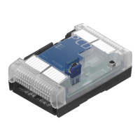
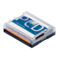
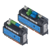
7 PCD2.B160 & PCD3.B160
7.1 Module Overview .................................................................................. 7-2
7.2 Hardware ............................................................................................... 7-2
7.2.1 I/O connection ....................................................................................... 7-3
7.2.2 LED signalization .................................................................................. 7-3
7.2.3 General technical data on inputs and outputs ....................................... 7-4
7.2.4 Technical data on inputs ........................................................................ 7-4
7.2.5 Input wiring ............................................................................................ 7-4
7.2.6 Technical data on outputs ..................................................................... 7-5
7.2.7 Output wiring ......................................................................................... 7-5
7.2.8 Label Editor ........................................................................................... 7-6
7.2.9 Bloc Diagram ......................................................................................... 7-7
7.3 CongurationinPG5deviceCongurator ............................................. 7-8
7.4 Media Mapping ...................................................................................... 7-10
7.4.1 Symbol name & description .................................................................. 7-10
7.4.1.1 RdDigitalIO ............................................................................................ 7-10
7.4.1.2 RdOutputError ....................................................................................... 7-10
7.4.1.3 WrDigitalOutput ..................................................................................... 7-10
7.5 Direct input or output access in IL ......................................................... 7-11
7.5.1 Symbol name & description ................................................................. 7-11
7.5.1.1 RD_DIGITAL_IO_0TO15 ....................................................................... 7-11
7.5.1.2 MASK_RD_DIGITALOUTPUT_0TO15 ................................................. 7-11
7.5.1.3 RD_OUTPUT_ERROR_0TO15 ............................................................ 7-12
7.5.1.4 RD_FIRMWARE_VERSION ................................................................ 7-12
7.5.1.5 RD_MODULE_STATUS ........................................................................ 7-13
7.5.1.6 WR_DIGITAL_OUTPUT_0TO15 ........................................................... 7-13
7.5.2. Error PCD XOB 13 ................................................................................ 7-14
7.6 Error PCD XOB 13 ................................................................................ 7-15
8 PCD2.W380 & PCD3.W380
8.1 PCD2/3.W380,8analogcongurableinputs ........................................ 8-2
8.1.1 Module overview ................................................................................... 8-2
8.1.2 Inputs connection .................................................................................. 8-3
8.1.3 Specications ........................................................................................ 8-4
8.1.3.1 General data ......................................................................................... 8-4
8.1.3.2 Technical data of inputs ......................................................................... 8-5
8.1.4 Input wiring ............................................................................................ 8-7
8.1.5 Input values acquisition ......................................................................... 8-8
8.1.6 Congurabledigitallters ...................................................................... 8-9
8.1.7 Out of range indication .......................................................................... 8-9
8.1.8 Input protections .................................................................................... 8-10
8.1.8.1 Current measuring range ...................................................................... 8-10
8.1.9 Protection mode .................................................................................... 8-11
8.1.10 LED signalization .................................................................................. 8-11
8.1.11 Block diagram ....................................................................................... 8-12
8.2 Preparing the PLC system .................................................................... 8-12