254
ABOV Semiconductor Co., Ltd.
11.13.4 USI0/1 Clock Generation
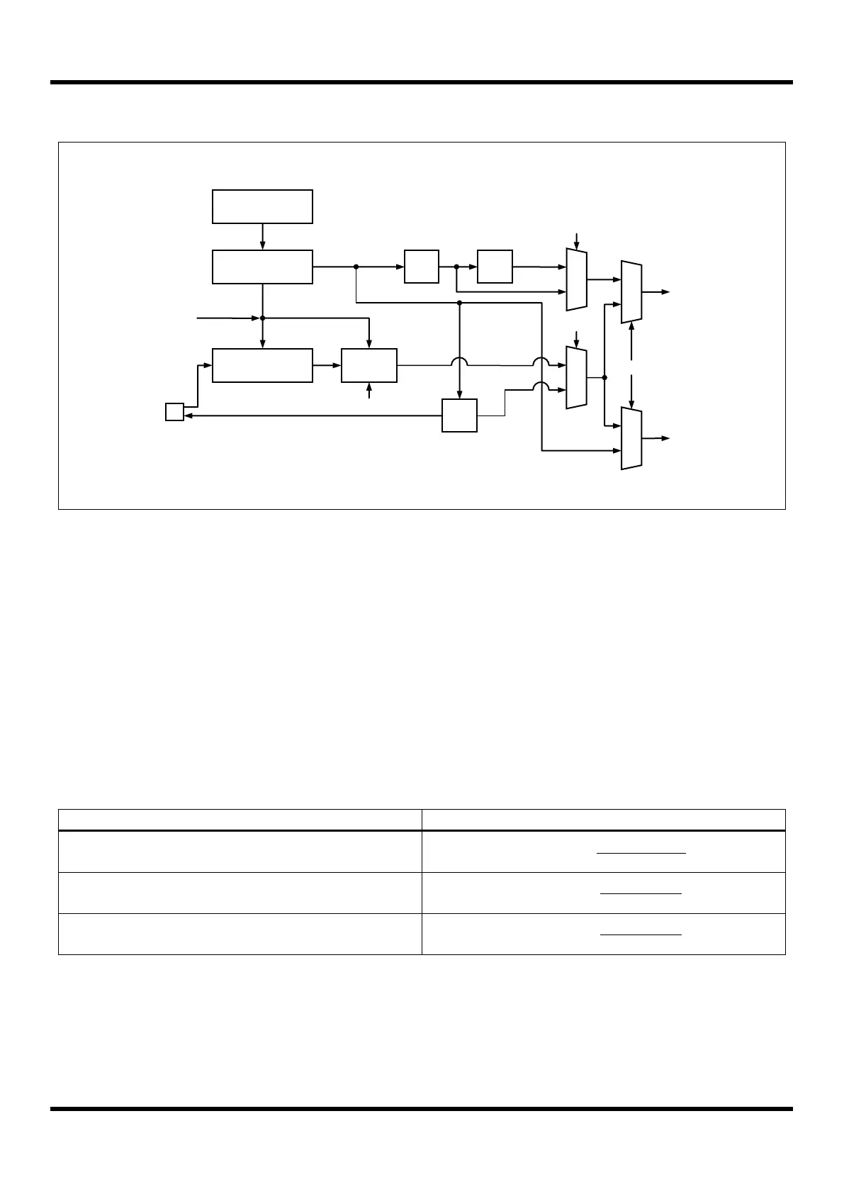
Figure 11.63 Clock Generation Block Diagram (USIn, where n = 0 and 1)
The clock generation logic generates the base clock for the transmitter and receiver. The USI0/1 supports four modes
of clock operation and those are normal asynchronous, double speed asynchronous, master synchronous and slave
synchronous mode. The clock generation scheme for master SPI and slave SPI mode is the same as master
synchronous and slave synchronous operation mode. The USInMS[1:0] bits in USInCR1 register selects
asynchronous or synchronous operation. Asynchronous double speed mode is controlled by the DBLSn bit in the
USInCR2 register. The MASTERn bit in USInCR3 register controls whether the clock source is internal (master mode,
output pin) or external (slave mode, input pin). The SCKn pin is active only when the USI0/1 operates in synchronous
or SPI mode.
Following table shows the equations for calculating the baud rate (in bps).
Equation for Calculating Baud Rate
Asynchronous Normal Mode (DBLSn=0)
Baud Rate =
fx
16(USInBD + 1)
Asynchronous Double Speed Mode (DBLSn=1)
Baud Rate =
fx
8(USInBD + 1)
Synchronous or SPI Master Mode
Baud Rate =
fx
2(USInBD + 1)
Table 11-22 Equations for Calculating USI0/1 Baud Rate Register Setting