350
ABOV Semiconductor Co., Ltd.
14.1.2 Feature
• Two-wire external interface: 1-wire serial clock input, 1-wire bi-directional serial data bus
• Debugger Access to:
− All Internal Peripheral Units
− Internal data RAM
− Program Counter
− Flash and Data EEPROM Memories
• Extensive On-chip Debug Support for Break Conditions, Including
− Break Instruction
− Single Step Break
− Program Memory Break Points on Single Address
− Programming of Flash, EEPROM, Fuses and Lock Bits through the two-wire Interface
− On-chip Debugging Supported by OCD dongle
• Operating frequency
• Supports the maximum frequency of the target MCU
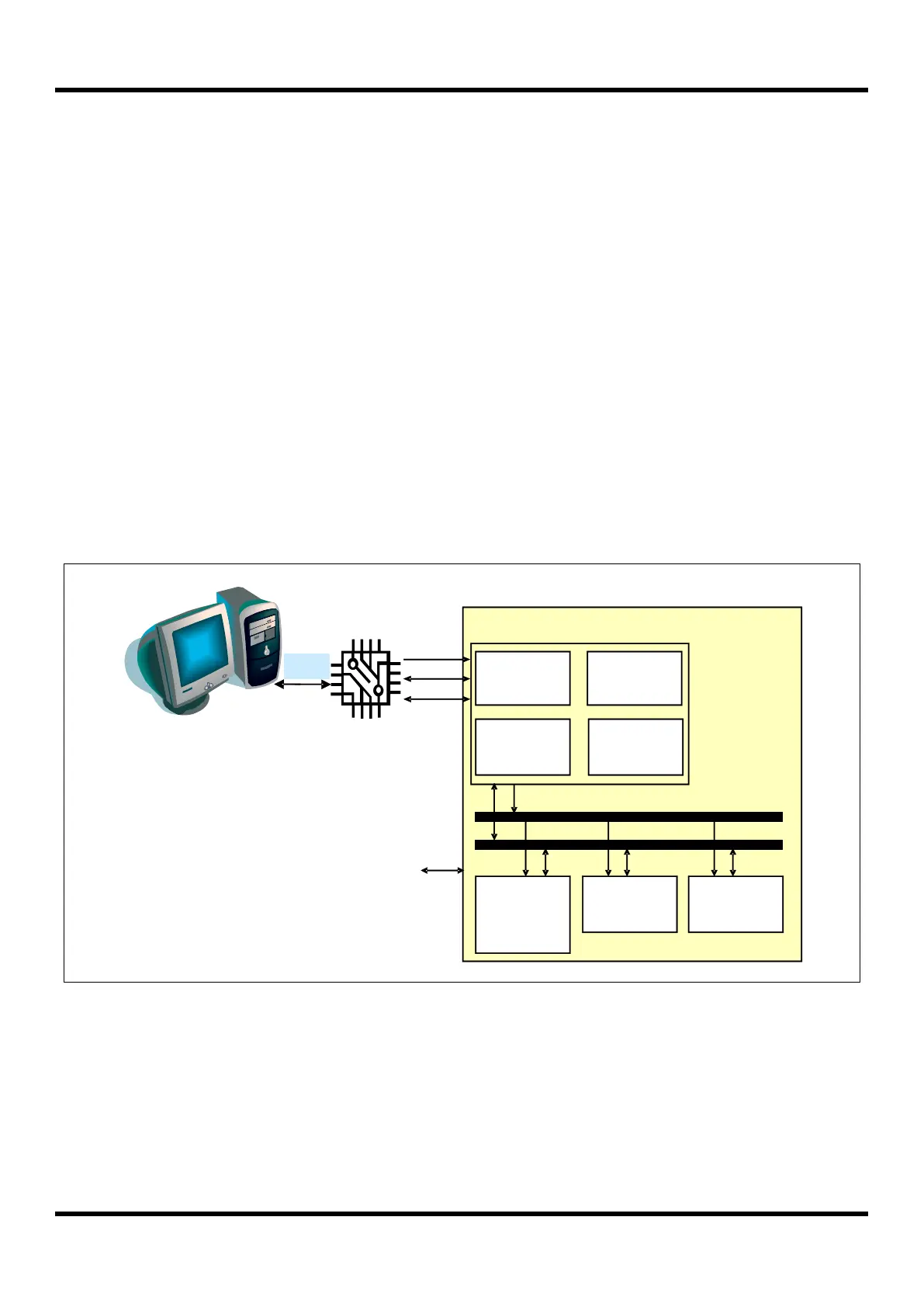
Figure 14.1 Block Diagram of On-Chip Debug System
Target MCU internal circuit