EasyManuals Logo

Abov MC97F60128 User Manual

Abov MC97F60128
382 pages
To Next Page IconTo Next Page
To Previous Page IconTo Previous Page
Page #40 background imageLoading...
Page #40 background image
40
MC97F60128
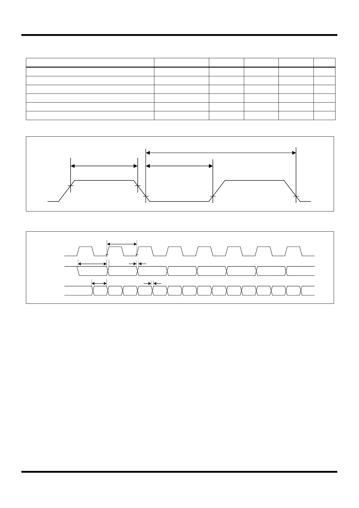
7.14 UART0/1/2/3/4 Characteristics
(T
A
=-40°C ~ +85°C, VDD=1.8V ~ 5.5V, f
XIN
=11.1MHz)
Parameter
Symbol
MIN
TYP
MAX
Unit
Serial port clock cycle time
t
SCK
1250
t
CPU
x 16
1650
ns
Output data setup to clock rising edge
t
S1
590
t
CPU
x 13
–
ns
Clock rising edge to input data valid
t
S2
–
–
590
ns
Output data hold after clock rising edge
t
H1
t
CPU
- 50
t
CPU
–
ns
Input data hold after clock rising edge
t
H2
0
–
–
ns
Serial port clock High, Low level width
t
HIGH
,t
LOW
470
t
CPU
x 8
970
ns
Table 7-15 UART0/1/2/3/4 Characteristics
t
HIGH
t
LOW
t
SCK
Figure 7.3 Waveform for UART0/1/2/3/4 Timing Characteristics
Shift Clock
Data Out D1 D2 D3 D4 D5 D6 D7D0
ValidData In Valid Valid Valid Valid Valid Valid Valid
tSCK
tS1
tH1
tH2
tS2
Figure 7.4 Timing Waveform for the UART0/1/2/3/4 Module

Table of Contents

Questions and Answers:

Question and Answer IconNeed help?

Do you have a question about the Abov MC97F60128 and is the answer not in the manual?

Abov MC97F60128 Specifications

General IconGeneral
BrandAbov
ModelMC97F60128
CategoryMicrocontrollers
LanguageEnglish

Related product manuals