36
ABOV Semiconductor Co., Ltd.
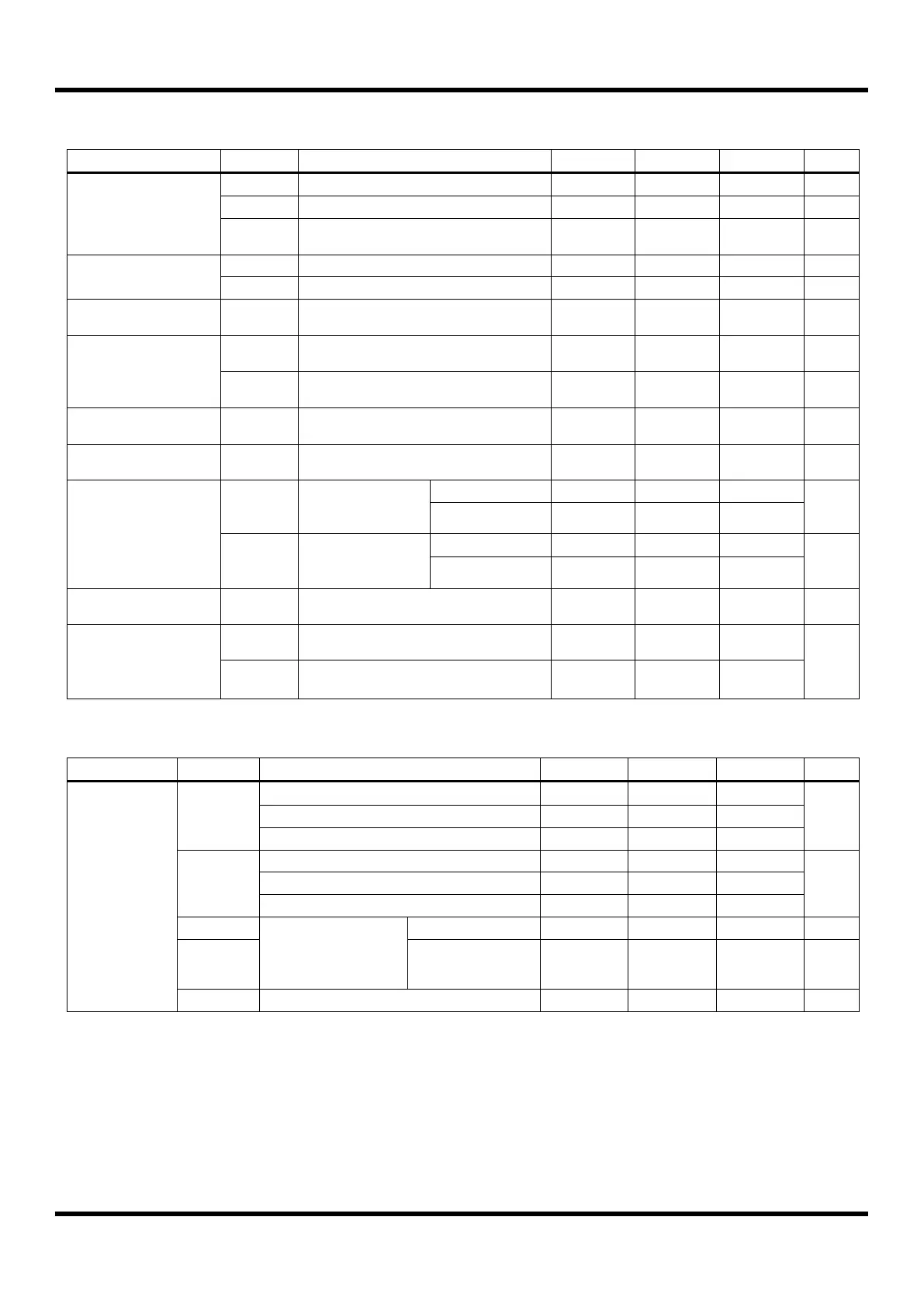
7.11 DC Characteristics
(T
A
= -40°C ~ +85°C, VDD= 1.8V ~ 5.5V, VSS= 0V, f
XIN
= 12MHz)
All input pins except VIH1
P20, P33, P34, P37;
3V Interface mode
All input pins except V
IL1
VDD=4.5V, I
OH
=-2mA,
All output ports;
VDD=4.5V, I
OL
= 10mA;
All output ports except V
OL2
VDD=4.5V, IOL=15mA;
P10–P13, P23–P24, P4
Input High Leakage
Current
Input Low Leakage
Current
VI=0V,
T
A
= 25°C
All Input ports
VDD= 5.0V, T
A
= 25°C
RUNFLAG
XIN= VDD, XOUT= VSS
T
A
= 25°C, VDD= 5V
SXIN=VDD, SXOUT=VSS
T
A
= 25°C, VDD=5V
Table 7-11 DC Characteristics
(T
A
= -40°C ~ +85°C, VDD= 1.8V ~ 5.5V, VSS= 0V)
f
XIN
=32.768kHz
VDD= 3V±10%
T
A
= 25°C,
PSAVE=1
STOP, VDD= 5V±10%, T
A
= 25°C
Table 7-12 DC Characteristics(Continued)
NOTE)
1. Where the fxin is an external main oscillator, the fSUB is an external sub oscillator, the fIRC is an
internal
RC oscillator, the fPLL is the output frequency of the PLL (phase locked-loop) and the fx is the
selected
system clock.