{ }
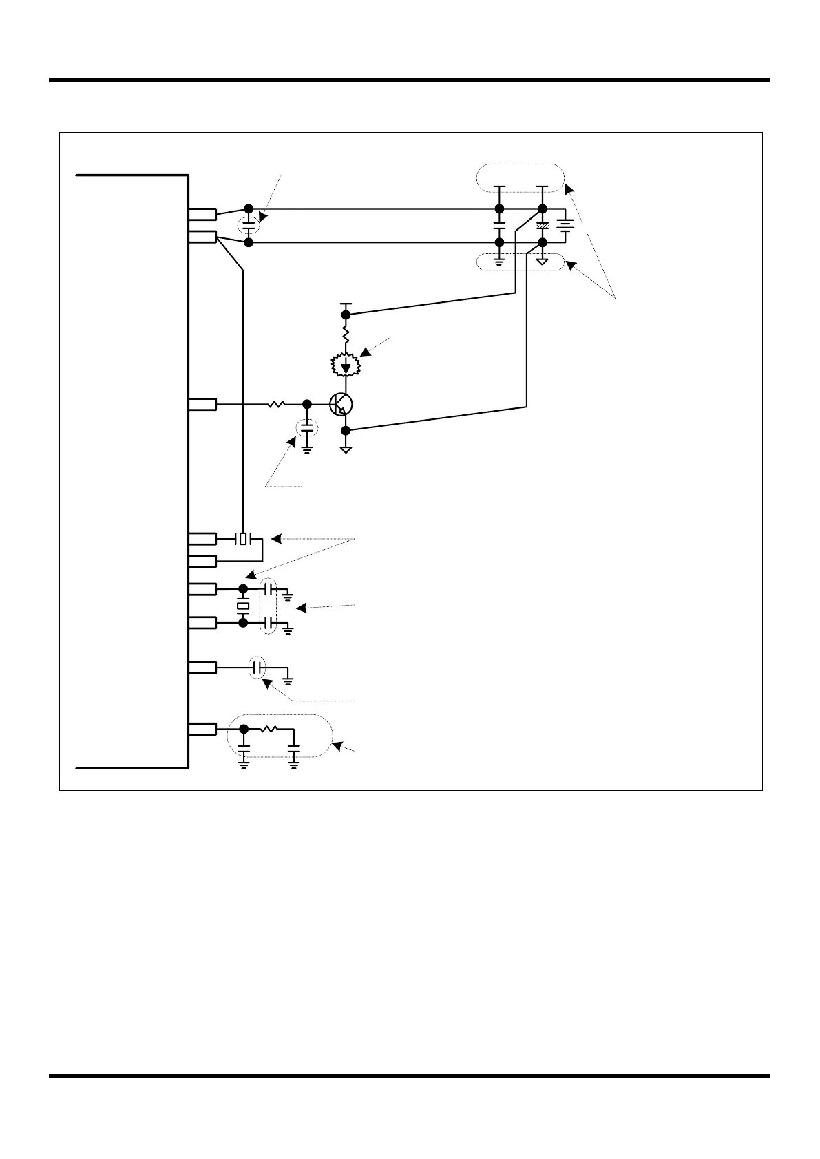
MC97F60128
XOUT
XIN
I/O
VSS1
VDD1
High-Current Part
Infrared LED,
FND(7-Segment),
,,,,,
etc
{ }
0.01uF
VCC
0.1uF
This 0.1uF capacitor should be within
1cm from the VDD pin of MCU on the
PCB layout.
{ }
This 0.01uF capacitor is alternatively
for noise immunity.
X-tal
SXOUT
SXIN
32.768kHz
The main and sub crystal should be within 1cm from the pins of MCU on the PCB layout.
VREG
0.1uF
The VREG pin is the output of an internal regulator for sub oscillator.
So, this 0.1uF capacitor is needed and should be as close by the MCU
as possible if the sub clock is used for system.
+
0.1uF
VDD VCC
{ }
The MCU power line (VDD and VSS)
should be separated from the high-
current part at a DC power node on
the PCB layout.
DC Power
The load capacitors of the sub clock
- C1, C2: CL x 2 ± 15%
- CL = (C1 x C2)/(C1 + C2) - Cstray
- CL: the specific capacitor value of crystal
- Cstray: the parasitic capacitor of a PCB (1pF – 1.5pF)
C1
C2
LPF
The LPF pin is the loop filter pump output for the PLL.
So, these parts should be as close by the MCU as possible if needed.
10nF820pF
6.8kΩ