32
ABOV Semiconductor Co., Ltd.
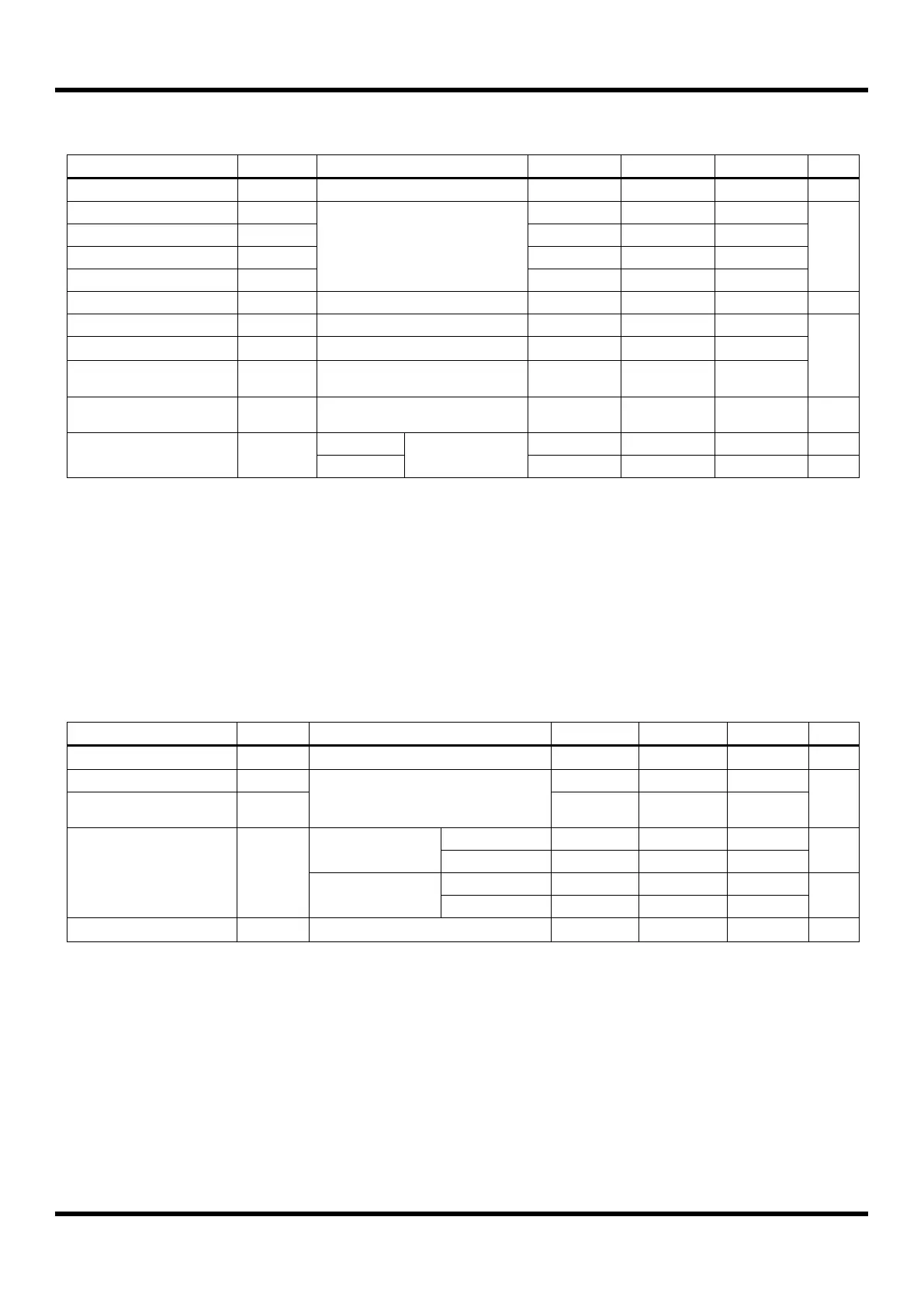
7.3 A/D Converter Characteristics
(T
A
= - 40
C to + 85
C, V
DD
= 1.8 – 5.5V, VDD = AVREF, VSS=AVSS=0V)
AVREF= 2.7V – 5.5V
fx= 8MHz
Differential Non-Linearity
Analog Input Leakage
Current
Table 7-3 A/D Converter Characteristics
NOTE)
1. Zero offset error is the difference between 000000000000 and the converted output for zero
input voltage (AVSS).
2. Top offset error is the difference between 111111111111 and the converted output for top input
voltage (AVREF).
3. When AVREF is lower than 2.7V, the ADC resolution is worse.
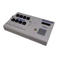
7.4 D/A Converter Characteristics
(T
A
= - 40
C to + 85
C, V
DD
= 1.8 – 5.5V, VDD , VSS=AVSS=0V)
VDD= 2.7V – 5.5V
fx= 8MHz
Differential Linearity
Error
Table 7-4 D/A Converter Characteristics