EasyManua.ls Logo

Abov MC97F60128 - Power-On Reset Characteristics; Low Voltage Reset and Low Voltage Indicator Characteristics; Phase Locked Loop Characteristics

Abov MC97F60128
382 pages
To Next Page IconTo Next Page
To Previous Page IconTo Previous Page
Loading...
33
MC97F60128
ABOV Semiconductor Co., Ltd.
7.5 Power-On Reset Characteristics
(T
A
=-40°C ~ +85°C, VDD=1.8V ~ 5.5V, VSS=0V)
Parameter
Symbol
Conditions
MIN
TYP
MAX
Unit
RESET Release Level
V
POR
1.4
V
VDD Voltage Rising Time
t
R
0.05
30.0
V/ms
POR Current
I
POR
0.2
uA
Table 7-5 Power-on Reset Characteristics
7.6 Low Voltage Reset and Low Voltage Indicator Characteristics
(T
A
=-40°C ~ +85°C, VDD=1.8V ~ 5.5V, VSS=0V)
Parameter
Symbol
Conditions
MIN
TYP
MAX
Unit
Detection Level
V
LVR
V
LVI
The LVR can select all levels but
LVI can select other levels except
1.60V
1.60
1.79
V
1.85
2.00
2.15
1.95
2.10
2.25
2.05
2.20
2.35
2.17
2.32
2.47
2.29
2.44
2.59
2.39
2.59
2.79
2.55
2.75
2.95
2.73
2.93
3.13
2.94
3.14
3.34
3.18
3.38
3.58
3.37
3.67
3.97
3.70
4.00
4.30
4.10
4.40
4.70
Hysteresis
V
50
150
mV
Minimum Pulse Width
t
LW
100
us
LVR and LVI Current
I
BL
Enable (Both)
VDD= 3V,
RUN Mode
14.0
24.0
uA
Enable (One of two)
10.0
18.0
Disable (Both)
VDD= 3V
0.1
Table 7-6 LVR and LVI Characteristics
7.7 Phase Locked Loop Characteristics
(T
A
=-40°C ~ +85°C, VDD=1.8V ~ 5.5V, VSS=0V)
Parameter
Symbol
Conditions
MIN
TYP
MAX
Unit
Input Frequency Range
C2
R
C1
LPFVSS
32.768
kHz
Output Frequency Range
f
VCO
1.024
8.192
MHz
Clock Duty Ratio
TOD
45
50
55
%
Tolerance
±4
%
Settling Time
t
D
10
100
ms
PLL Current
I
PLL
Enable, fVCO=8.192MHz
0.5
1.0
mA
Disable
0.1
uA
Table 7-7 Phase Locked Loop Characteristics
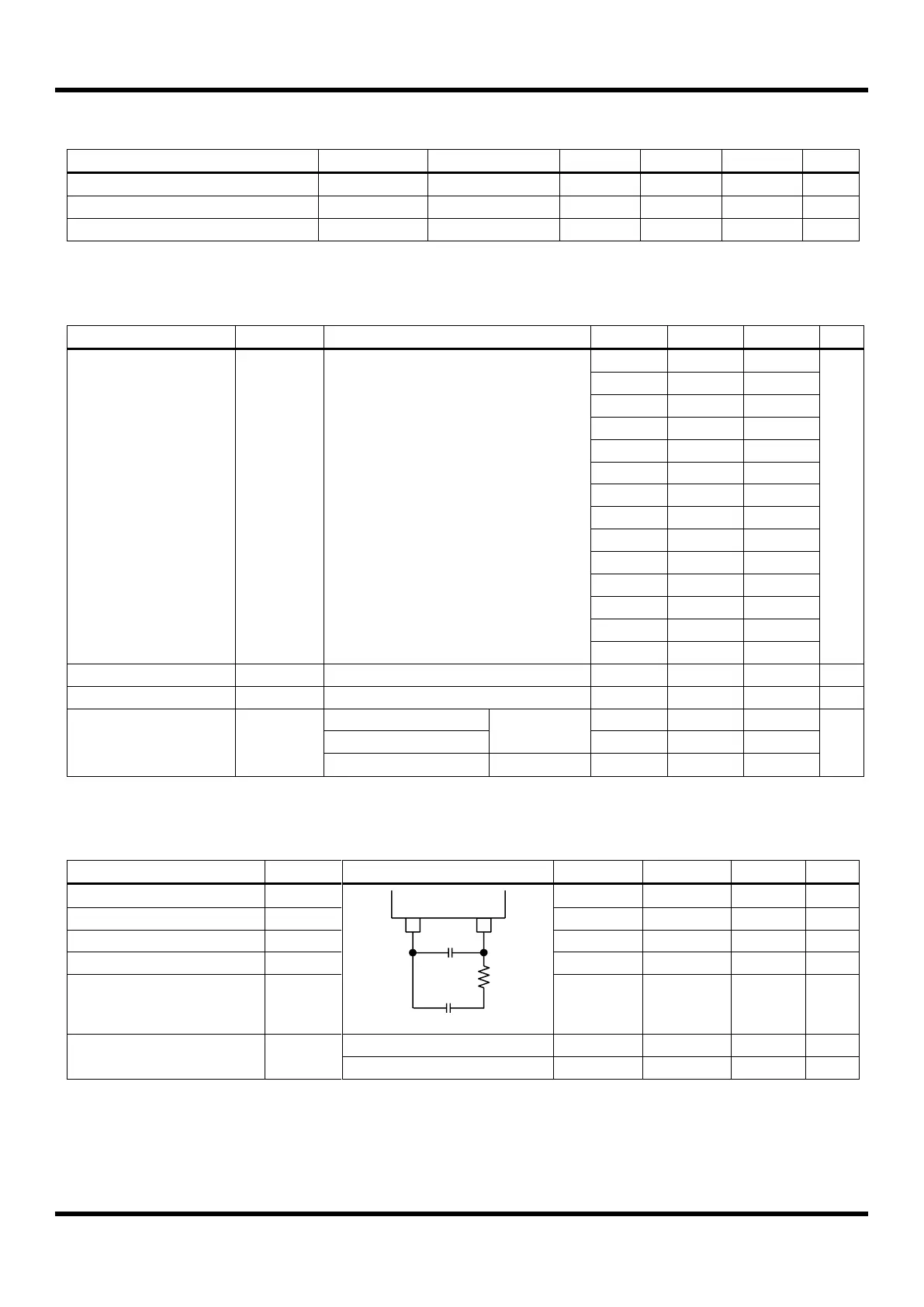
NOTE)
1. Where R= 6.8kΩ, C1=820pF and C2= 10nF.

Table of Contents

Related product manuals