Home
Abov
Microcontrollers
MC97F60128
Abov MC97F60128 User Manual
4
of 1
of 1 rating
382 pages
Give review
Manual
Specs
To Next Page
To Next Page
To Previous Page
To Previous Page
Loading...
44
MC97F60128
A
BOV Semiconductor Co., Ltd.
7.19
Main Clock Oscillat
or Characteristics
(T
A
=-
40
°
C ~ +85
°
C,
VDD=1.8V ~ 5.5
V)
Oscillator
Parameter
Condition
MIN
TYP
MAX
Unit
Crystal
Main oscillation frequency
2.0
V
–
5.5V
0.4
–
4.2
MHz
2.7V
–
5.5V
0.4
–
12
.0
Ceramic Oscillator
Main oscillation frequency
1.8
V
–
5.5V
0.4
–
4.2
MHz
2.7V
–
5.5V
0.4
–
12
.0
External Clock
XIN input frequency
1.8
V
–
5.5V
0.4
–
4.2
MHz
2.7V
–
5.5V
0.4
–
12
.0
Table 7-
20
Main Clock Oscillator Characteristics
XIN
XOUT
C1
C2
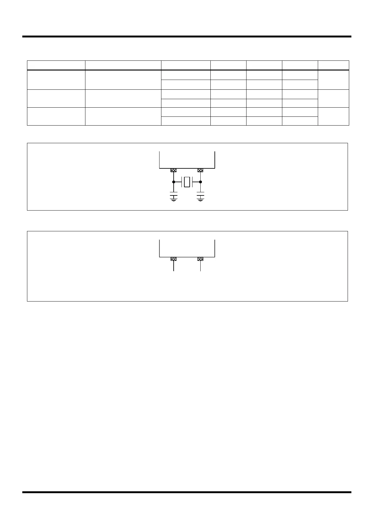
Figure 7.8
Crystal/Ceramic Oscillator
XIN
XOUT
External
Clock
Source
Open
Figure 7.9
External Clock
43
45
Table of Contents
Revision History
2
1 Overview
4
Description
4
Features
5
Development Tools
7
Compiler
7
Ocd2(On-Chip Debugger) Emulator and Debugger
7
Programmer
8
MTP Programming
10
Overview
10
On-Board Programming
10
Circuit Design Guide
11
2 Block Diagram
12
3 Pin Assignment
13
4 Package Diagram
17
5 Pin Description
21
6 Port Structures
29
General Purpose I/O Port
29
External Interrupt I/O Port
30
7 Electrical Characteristics
31
Absolute Maximum Ratings
31
Recommended Operating Conditions
31
A/D Converter Characteristics
32
D/A Converter Characteristics
32
Power-On Reset Characteristics
33
Low Voltage Reset and Low Voltage Indicator Characteristics
33
Phase Locked Loop Characteristics
33
Internal RC Oscillator Characteristics
34
Internal Watch-Dog Timer RC Oscillator Characteristics
34
LCD Voltage Characteristics
35
DC Characteristics
36
AC Characteristics
38
SPI0/1/2/3 Characteristics
39
UART0/1/2/3/4 Characteristics
40
I2C0/1 Characteristics
41
Data Retention Voltage in Stop Mode
42
Internal Flash Rom Characteristics
43
Input/Output Capacitance
43
Main Clock Oscillator Characteristics
44
Sub Clock Oscillator Characteristics
45
Main Oscillation Stabilization Characteristics
46
Sub Oscillation Characteristics
46
Operating Voltage Range
47
Recommended Circuit and Layout
48
Recommended Circuit and Layout with SMPS Power
49
Typical Characteristics
50
8 Memory
53
Program Memory
53
Data Memory
55
External Data Memory
57
SFR Map
58
SFR Map Summary
58
SFR Map
60
SFR Map
71
9 I/O Ports
77
Port Register
77
Data Register (Px)
77
Direction Register (Pxio)
77
Pull-Up Resistor Selection Register (Pxpu)
77
Open-Drain Selection Register (Pxod)
77
Debounce Enable Register (Pxdb)
77
Port Function Selection Register (Pxfsr)
78
Register Map
78
P0 Port
80
P0 Port Description
80
Register Description for P0
80
P1 Port
83
P1 Port Description
83
Register Description for P1
83
P2 Port
87
P2 Port Description
87
Register Description for P2
87
P3 Port
90
P3 Port Description
90
Register Description for P3
90
P4 Port
93
P4 Port Description
93
Register Description for P4
93
P5 Port
97
P5 Port Description
97
Register Description for P5
97
P6 Port
100
P6 Port Description
100
Register Description for P6
100
P7 Port
103
P7 Port Description
103
Register Description for P7
103
P8 Port
106
P8 Port Description
106
Register Description for P8
106
P9 Port
108
P9 Port Description
108
Register Description for P9
108
PA Port
111
PA Port Description
111
Register Description for PA
111
PB Port
114
PB Port Description
114
Register Description for PB
114
PD Port
116
PD Port Description
116
Register Description for PD
116
10 Interrupt Controller
118
Overview
118
External Interrupt
119
Block Diagram
120
Interrupt Vector Table
121
Interrupt Sequence
122
Effective Timing after Controlling Interrupt Bit
123
Multi Interrupt
124
Interrupt Enable Accept Timing
125
Interrupt Service Routine Address
125
Saving/Restore General-Purpose Registers
125
Interrupt Timing
126
Interrupt Register Overview
126
Interrupt Enable Register (IE, IE1, IE2, IE3)
126
Interrupt Priority Register (IP, IP1)
126
External Interrupt Flag Register (EIFLAG0, EIFLAG1)
127
External Interrupt Polarity Register (EIPOL0L, EIPOL0H, EIPOL1)
127
Register Map
127
Interrupt Register Description
128
Register Description for Interrupt
129
11 Peripheral Hardware
140
Clock Generator
140
Overview
140
Block Diagram
141
Phase Locked-Loop Block Diagram
141
Register Map
142
Clock Generator Register Description
142
Register Description for Clock Generator
142
Basic Interval Timer
145
Overview
145
Block Diagram
145
Register Map
146
Basic Interval Timer Register Description
146
Register Description for Basic Interval Timer
146
Watch Dog Timer
148
Overview
148
WDT Interrupt Timing Waveform
148
Block Diagram
149
Register Map
149
Watch Dog Timer Register Description
149
Register Description for Watch Dog Timer
150
Watch Timer
151
Overview
151
Block Diagram
151
Register Map
152
Watch Timer Register Description
152
Register Description for Watch Timer
152
Timer 0/1/2
154
Overview
154
8-Bit Timer/Counter Mode
155
8-Bit PWM Mode
156
8-Bit Capture Mode
158
Block Diagram
160
Register Map
161
Timer/Counter 0/1/2 Register Description
161
Register Description for Timer/Counter 0/1/2
161
Timer 3/4/5/6
165
Overview
165
16-Bit Timer/Counter Mode
165
16-Bit Capture Mode
167
16-Bit PPG Mode
169
Block Diagram
171
Register Map
172
Timer/Counter 3/4/5/6 Register Description
172
Register Description for Timer/Counter 3/4/5/6
173
Timer 7/8
176
Overview
176
8-Bit Timer/Counter 7/8 Mode
177
16-Bit Timer/Counter 7 Mode
178
8-Bit Timer 7/8 Capture Mode
179
16-Bit Timer 7 Capture Mode
181
10-Bit Timer 8 PWM Mode
182
Block Diagram
193
Register Map
195
Timer/Counter 7 Register Description
196
Register Description for Timer/Counter 7
196
Timer/Counter 8 Register Description
198
Register Description for Timer/Counter 8
198
10-Bit PWM Generator
206
Overview
206
Function Description
206
10-Bit PWM One-Shot Mode Without Auto-Enable
207
10-Bit PWM One-Shot Mode with Auto-Enable
208
10-Bit PWM Repeat Mode
209
Timing Chart of the Valid Falling Edge by an External Pin
210
Block Diagram
212
Register Map
213
10-Bit PWM Generator Register Description
213
Register Description for 10-Bit PWM Generator
214
Buzzer Driver
219
Overview
219
Overview
220
Register Map
221
Buzzer Driver Register Description
221
Register Description for Buzzer Driver
221
Spi 2
222
Overview
222
Block Diagram
222
Data Transmit / Receive Operation
223
SS2 Pin Function
223
SPI 2 Timing Diagram
224
Register Map
225
SPI 2 Register Description
225
Register Description for SPI 2
225
Spi 3
230
Overview
230
Block Diagram
230
Data Transmit / Receive Operation
231
SS3 Pin Function
231
SPI 3 Timing Diagram
232
Register Map
233
SPI 3 Register Description
233
Register Description for SPI 3
233
Uart2/3/4
236
Overview
236
Block Diagram
237
Clock Generation
238
Data Format
239
Parity Bit
240
UART2/3/4 Transmitter
240
Sending Tx Data
240
Transmitter Flag and Interrupt
240
Parity Generator
241
Disabling Transmitter
241
UART Receiver
241
Receiving Rx Data
241
Receiver Flag and Interrupt
242
Parity Checker
242
Disabling Receiver
242
Asynchronous Data Reception
243
Register Map
245
UART Register Description
245
Register Description for UART2/3/4
245
Baud Rate Setting (Example)
250
Usi0/1 (Uart + Spi + I2C)
251
Overview
251
USI0/1 UART Mode
252
USI0/1 UART Block Diagram
253
USI0/1 Clock Generation
254
USI0/1 External Clock (Sckn)
255
USI0/1 Synchronous Mode Operation
255
USI0/1 UART Data Format
256
USI0/1 UART Parity Bit
257
USI0/1 UART Transmitter
257
USI0/1 UART Sending Tx Data
257
USI0/1 UART Transmitter Flag and Interrupt
257
USI0/1 UART Parity Generator
258
UART Disabling Transmitter
258
USI0/1 UART Receiver
258
USI0/1 UART Receiving Rx Data
258
USI0/1 UART Receiver Flag and Interrupt
259
USI0/1 UART Parity Checker
259
USI0/1 UART Disabling Receiver
259
USI0/1 Asynchronous Data Reception
260
USI0/1 SPI Mode
262
USI0/1 SPI Clock Formats and Timing
262
USI0/1 SPI Block Diagram
265
USI0/1 I2C Mode
266
USI0/1 I2C Bit Transfer
266
USI0/1 I2C Start / Repeated Start / Stop
267
USI0/1 I2C Data Transfer
267
USI0/1 I2C Acknowledge
268
USI0/1 I2C Synchronization / Arbitration
268
USI0/1 I2C Operation
269
USI0/1 I2C Master Transmitter
270
USI0/1 I2C Master Receiver
272
USI0/1 I2C Slave Transmitter
274
USI0/1 I2C Slave Receiver
275
USI0/1 I2C Block Diagram
276
Register Map
277
Register Description
277
Register Description for USI0/1
277
Baud Rate Setting (Example)
286
12-Bit A/D Converter
287
Overview
287
Conversion Timing
287
Block Diagram
288
ADC Operation
289
Register Map
290
ADC Register Description
290
Register Description for ADC
291
12-Bit D/A Converter
294
Overview
294
Function Description
294
D/A Converter Data and Buffer Registers
294
Automatically D/AC Data Increment/Decrement
295
Programmable Gain Controller
296
12-Bit External D/AC Interface
297
Block Diagram
298
Register Map
299
DAC Register Description
299
Register Description for DAC
300
LCD Driver
304
Overview
304
LCD Display RAM Organization
305
LCD Signal Waveform
306
LCD Voltage Dividing Connection
310
Lcd Automatic Bias Control
313
Block Diagram
314
Register Map
315
LCD Driver Register Description
315
Register Description for LCD Driver
315
The Fine ADPCM Decoder
319
Overview
319
Function Description
319
The Decoder Result Output of the FADPCM
320
Serial Flash Interface by SPI2 or SPI3
321
Voice Prompt Play
322
Block Diagram
324
Register Map
325
FADPCM Register Description
325
Register Description for FADPCM
326
12 Power down Operation
332
Overview
332
Peripheral Operation in IDLE/STOP Mode
332
IDLE Mode
333
STOP Mode
334
Release Operation of STOP Mode
335
Register Map
336
Power down Operation Register Description
336
Register Description for Power down Operation
336
13 Reset
337
Overview
337
Reset Source
337
RESET Block Diagram
337
RESET Noise Canceller
338
Power on RESET
339
External RESETB Input
342
Brown out Detector Processor
343
LVI Block Diagram
344
Register Map
345
Reset Operation Register Description
345
Register Description for Reset Operation
346
14 On-Chip Debug System
349
Overview
349
Description
349
Feature
350
Two-Pin External Interface
351
Basic Transmission Packet
351
Packet Transmission Timing
352
Data Transfer
352
Bit Transfer
352
Start and Stop Condition
353
Acknowledge Bit
353
Connection of Transmission
354
Circuit
354
15 Flash Memory
355
Overview
355
Description
355
Flash Program ROM Structure
356
Register Map
357
Register Description for Flash Memory Control and Status
357
Register Description for Flash
358
Serial In-System Program (ISP) Mode
360
Protection Area (User Program Mode)
360
Erase Mode
361
Write Mode
362
Protection for Invalid Erase/Write
364
Flow of Protection for Invalid Erase/Write
366
Read Mode
367
Code Write Protection Mode
367
16 Configure Option
368
Configure Option Control
368
17 Appendix
369
Instruction Table
369
Flash Protection for Invalid Erase/Write
373
4
Based on 1 rating
Ask a question
Give review
Questions and Answers:
Need help?
Do you have a question about the Abov MC97F60128 and is the answer not in the manual?
Ask a question
Abov MC97F60128 Specifications
General
Brand
Abov
Model
MC97F60128
Category
Microcontrollers
Language
English
Related product manuals
Abov MC97F6108A
256 pages
Abov MC96F6432Q
327 pages
Abov MC96F6332D
327 pages
Abov MC96F6432 Series
327 pages
Abov A31G213CLN
29 pages