255
ABOV Semiconductor Co., Ltd.
11.13.5 USI0/1 External Clock (SCKn)
External clocking is used in the synchronous mode of operation.
External clock input from the SCKn pin is sampled by a synchronization logic to remove meta-stability. The output from
the synchronization logic must be passed through an edge detector before it is used by the transmitter and receiver.
This process introduces two CPU clock period delay. The maximum frequency of the external SCKn pin is limited up-
to 1MHz.
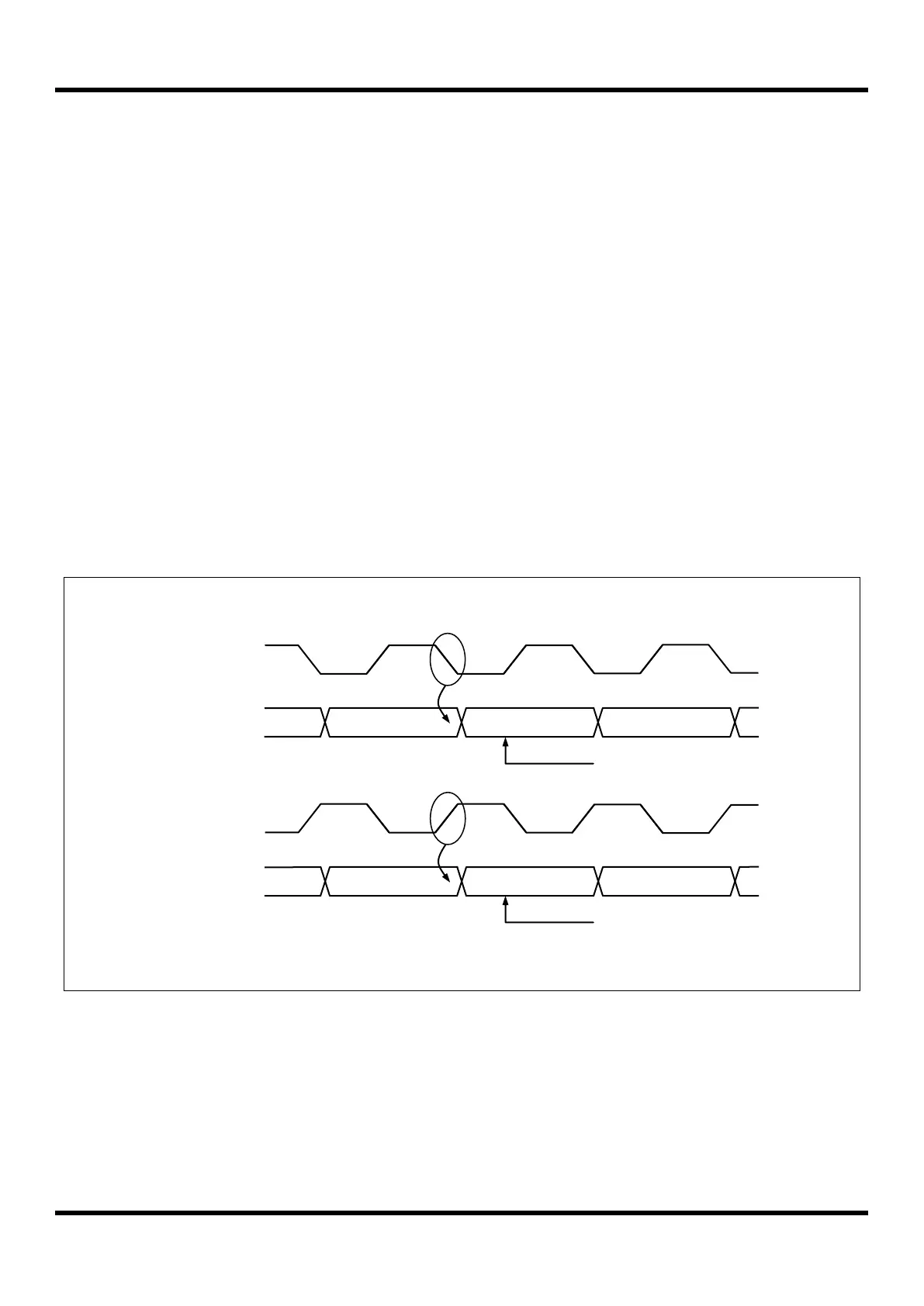
11.13.6 USI0/1 Synchronous mode operation
When synchronous or SPI mode is used, the SCKn pin will be used as either clock input (slave) or clock output
(master). Data sampling and transmitter is issued on the different edge of SCKn clock each other. For example, if data
input on RXDn (MISOn in SPI mode) pin is sampled on the rising edge of SCKn clock, data output on TXDn (MOSIn in
SPI mode) pin is altered on the falling edge.
The CPOLn bit in USInCR1 register selects which SCKn clock edge is used for data sampling and which is used for
data change. As shown in the figure below, when CPOLn is zero, the data will be changed at rising SCKn edge and
sampled at falling SCKn edge.
Figure 11.64 Synchronous Mode SCKn Timing (USIn , where n = 0 and 1)