28
ABOV Semiconductor Co., Ltd.
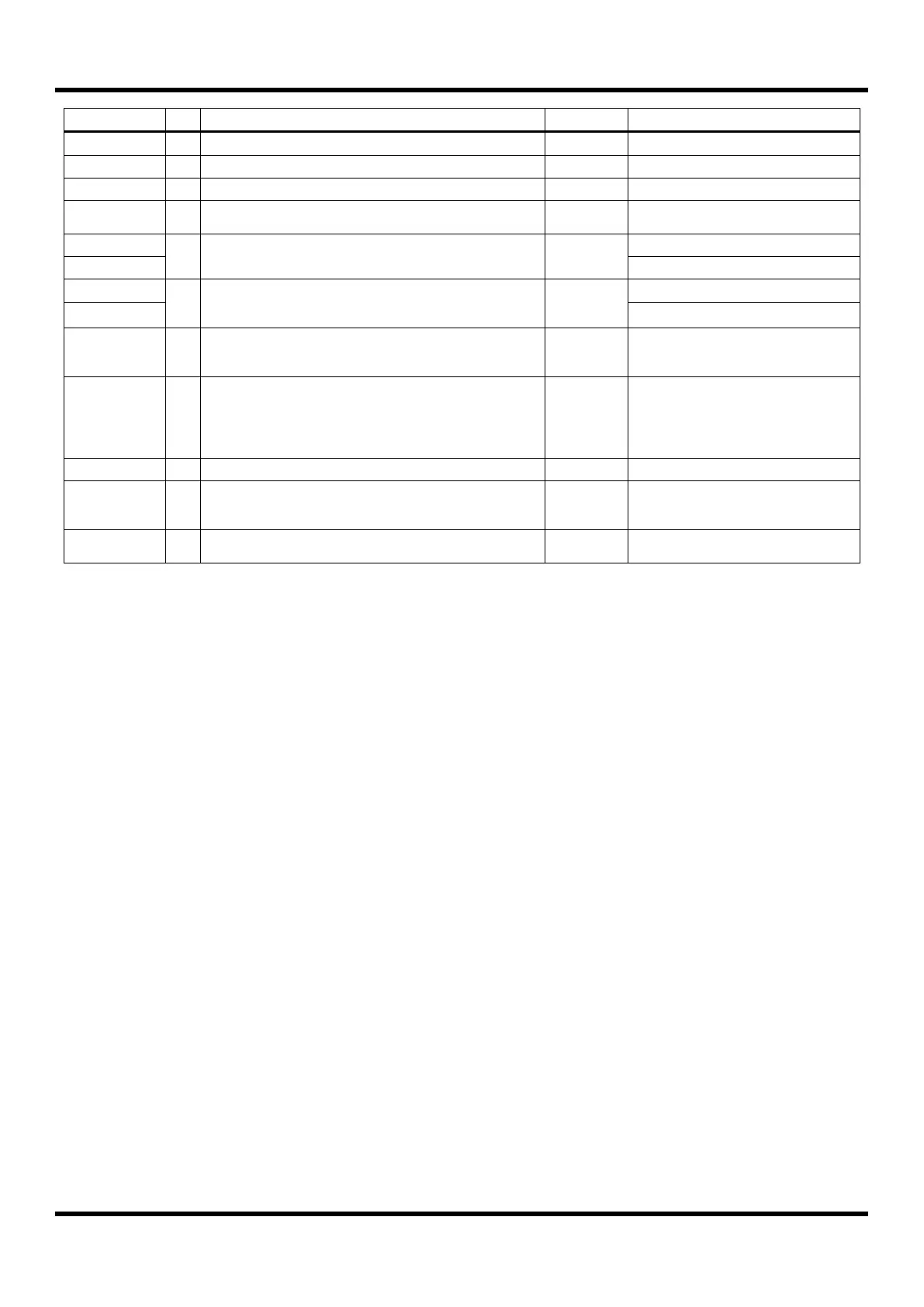
System reset pin with a pull-up resistor
On chip debugger data input/output
(Note 4)
On chip debugger clock input
(Note 4)
On chip debugger run flag
(Note 4)
with a pull-down
resistor
Sub oscillator pins
(Note 6)
The SXIN/SXOUT are not in the 64-Pin
(MC97F66128LB14) package.
Loop filter pump output for PLL
(Note 6)
The LPF are not in the 64-Pin (MC97F66128LB14)
package.
Regulator voltage output for sub clock
(Note 7)
0.1uF capacitor needed
Loop filter pump output for PLL
The VREG are not in the 64-Pin
(MC97F66128LB14) package.
A/D converter reference voltage
Analog power input pins
The AVSS are not in the 64-Pin (MC97F66128LB14)
package.
Table 5-8 Normal Pin Description (Continued)
NOTE)
1. The P9, PA, PB and PD pins are not in the 64(MC97F67128LB14)/80-pin package.
2. The P06-P07, P20-P23, P36-P37 and P8 pins are not in the 64-pin(MC97F67128LB14)
package.
3. The P20-P23, P36-P37, P8, P91-P94, PA2-PA4, PB and PD pins are not in the
64-pin(MC97F66128LB14) package.
4. If the P14/SEG62/EINT8/EC5/DSCL, P15/SEG63/EINT9/EC6/DSDA and RUNFLAG pins are
connected to an emulator, the pins are automatically configured as the debugger pins.
5. The P17/XOUT and P16/XIN pins are configured as a function pin by software control.
6. Do not connect if you do not use the SXIN, SXOUT and LPF.
7. Even if VREG is not used, 0.1uF capacitor Connect to between VREG and VSS.