157
8331B–AVR–03/12
Atmel AVR XMEGA AU
• Bit 4 – USART0: USART0 Remap
Setting this bit to one will move the pin location of USART0 from Px[3:0] to Px[7:4].
• Bit 3 – TC0D: Timer/Counter 0 Output Compare D
Setting this bit will move the location of OC0D from Px3 to Px7.
• Bit 2 – TC0C: Timer/Counter 0 Output Compare C
Setting this bit will move the location of OC0C from Px2 to Px6.
• Bit 1 – TC0B: Timer/Counter 0 Output Compare B
Setting this bit will move the location of OC0B from Px1 to Px5. If this bit is set and PWM from
both timer/counter 0 and timer/counter 1 is enabled, the resulting PWM will be an OR-modula-
tion between the two PWM outputs.
• Bit 0 – TC0A: Timer/Counter 0 Output Compare A
Setting this bit will move the location of OC0A from Px0 to Px4. If this bit is set and PWM from
both timer/counter 0 and timer/counter 1 is enabled, the resulting PWM will be an OR-modula-
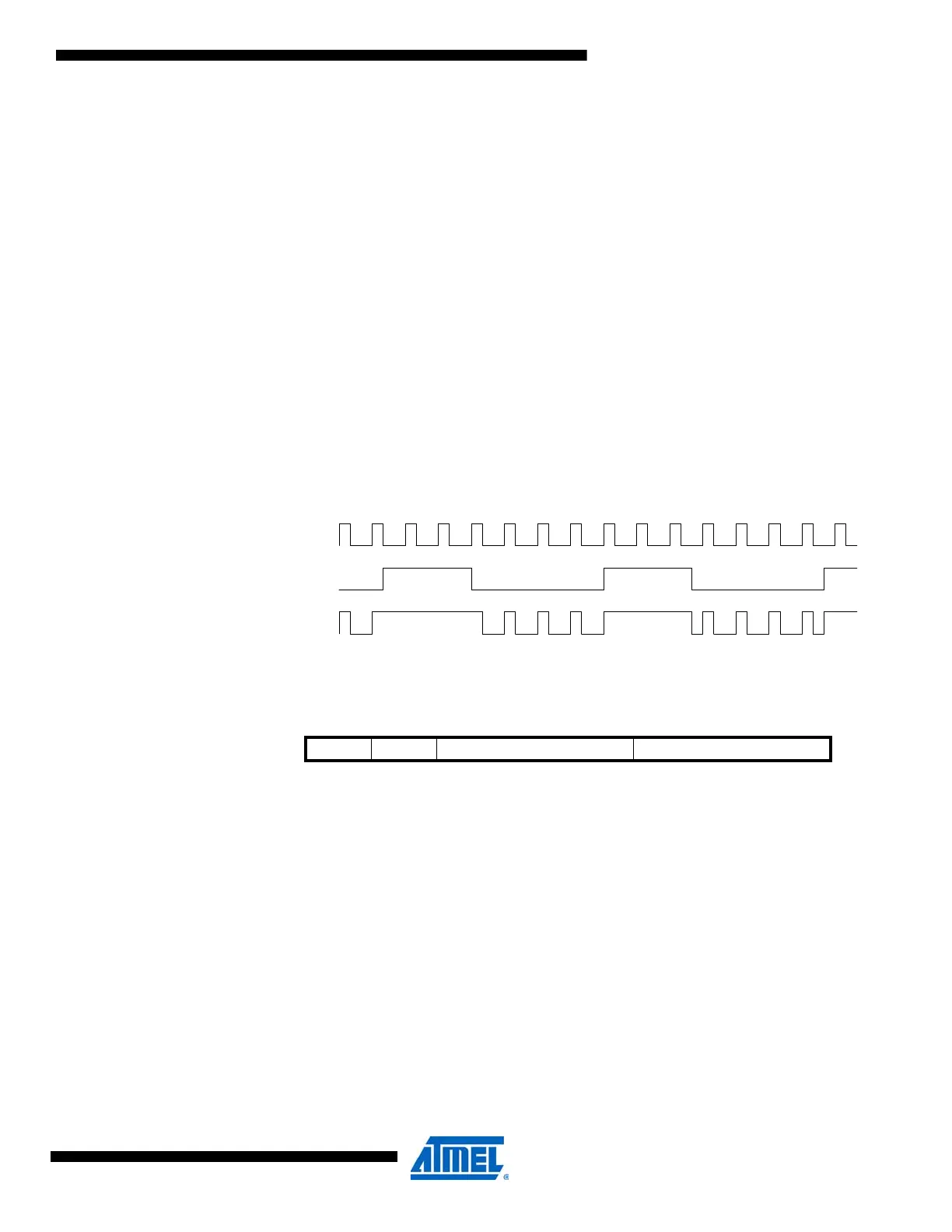
tion between the two PWM outputs. See Figure 13-11.
Figure 13-11. I/O timer/counter.
13.13.15 PINnCTRL – Pin n Configuration Register
• Bit 7 – SRLEN: Slew Rate Limit Enable
Setting this bit will enable slew rate limiting on pin n.
• Bit 6 – INVEN: Inverted I/O Enable
Setting this bit will enable inverted output and input data on pin n.
• Bit 5:3 – OPC: Output and Pull Configuration
These bits set the output/pull configuration on pin n according to Table 13-5.
Bit 76543210
SRLEN INVEN OPC[2:0] ISC[2:0] PINnCTRL
Read/Write R/W R/W R/W R/W R/W R/W R/W R/W
Initial Value00000000

 Loading...


