338
8331B–AVR–03/12
Atmel AVR XMEGA AU
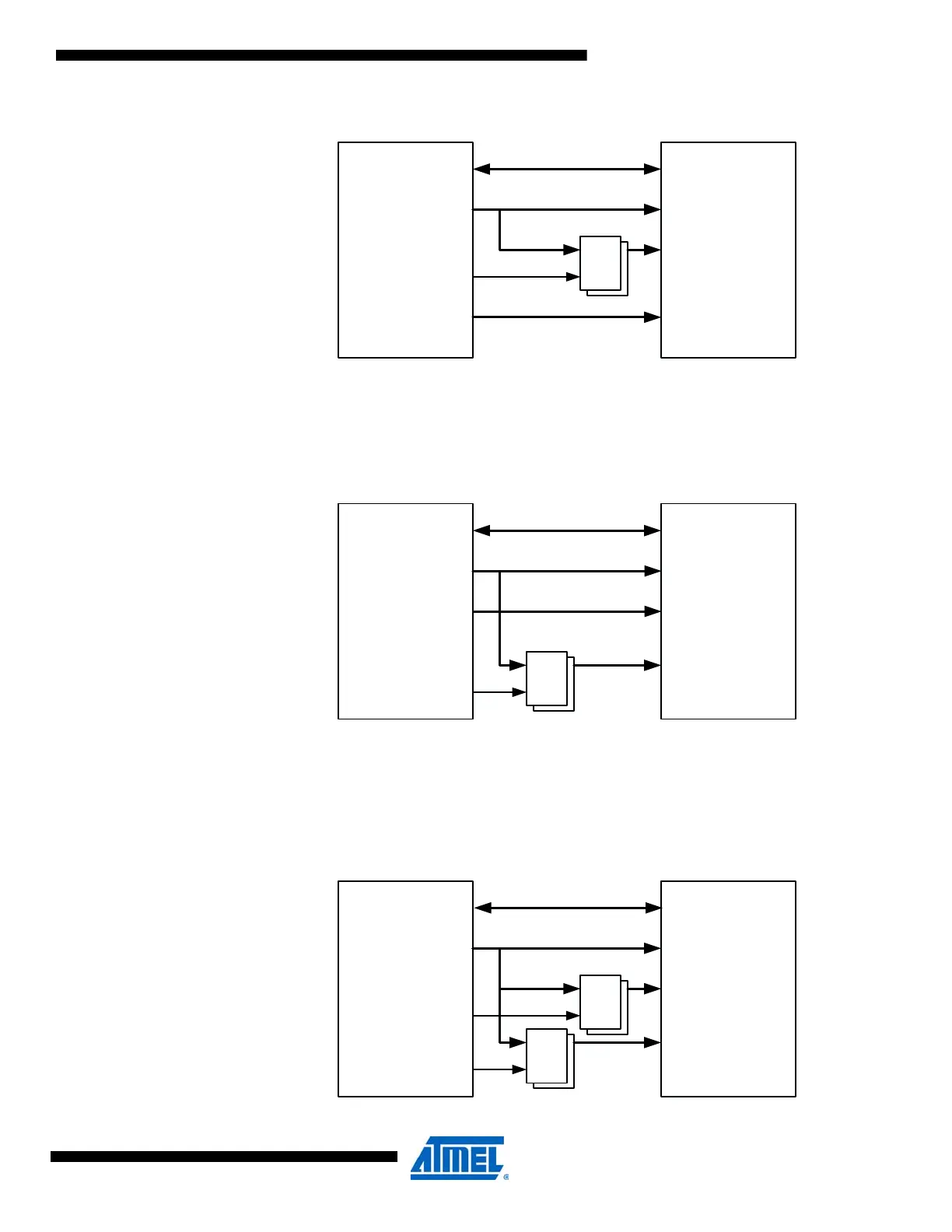
Figure 27-4. Multiplexed SRAM connection using ALE1.
27.5.3 Multiplexing address byte 0 and 2
When address byte 0 (A[7:0]) and address byte 2 (A[23:16) are multiplexed, they are output
from the same port, and the ALE2 signal from the device controls the address latch.
Figure 27-5. Multiplexed SRAM connection using ALE2.
27.5.4 Multiplexing address byte 0, 1and 2
When address byte 0 (A[7:0]), address byte 1 (A[15:8]) and address byte 2 (A[23:16] are multi-
plexed, they are output from the same port, and the ALE1 and ALE2 signal from the device
control the external address latches.
Figure 27-6. Multiplexed SRAM connection using ALE1 and ALE2.
EBI
SRAM
D[7:0]
A[15:8]/
A[7:0]
ALE1
D
Q
G
D[7:0]
A[7:0]
A[15:8]
A[19:16]
A[19:16]
EBI
SRAM
D[7:0]
A[23:16]/
A[7:0]
ALE2
D
Q
G
D[7:0]
A[7:0]
A[15:8]
A[23:16]
A[15:8]
EBI
SRAM
D[7:0]
A[23:16]/
A[15:8]/
A[7:0]
ALE1
ALE2
D
Q
G
D
Q
G
D[7:0]
A[7:0]
A[15:8]
A[23:16]

 Loading...


