493
8331B–AVR–03/12
Atmel AVR XMEGA AU
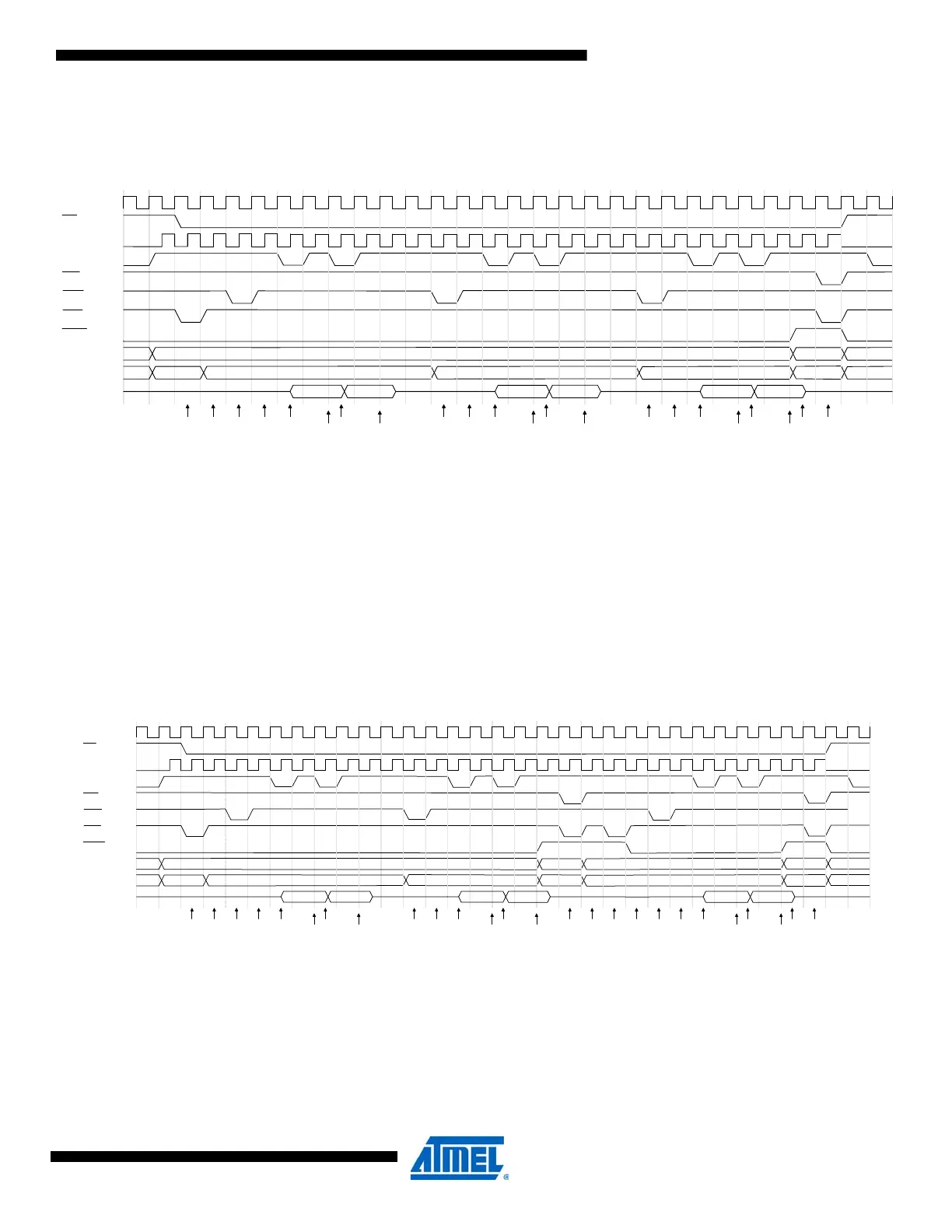
Figure 36-50. Burst access within a single page
Figure 36-51. Burst access crossing page boundary
** NOP is only inserted for CAS3
**** The number of NOPs is equal to WRDLY[1:0] + 1 (WRDLY = 0 is shown)
***** The number of NOPs is equal to RPDLY[1:0] (RPDLY = 1 is shown)
* The number of NOPs is equal to ROWCOLDLY[2:0] (ROWCOLDLY = 1 is shown)
*** Clock suspended for 1 cycle when EBI is running at 1x and 1 or 2 cycles when EBI
is running at 2x, to enable sampling of data on the positive edge of the 1x clock.
Bank Adr
Row Adr Col Adr
Burst access within a single page
0x0
Col Adr 0x400
Col Adr
Precharge All Banks
Active
Read
NOP*
NOP****
Data sampled
NOP**
Clock
suspend***
Read
Data sampled
NOP**
Clock
suspend***
Read
Data sampled
NOP**
Clock
suspend***
D[3:0] D[7:4]
Data sampled
Clock suspend
Data sampled
Clock suspend
D[3:0] D[7:4] D[3:0] D[7:4]
Data sampled
Clock suspend
CLK
CKE
CAS
RAS
DQM
BA[1:0]
A[11:0]
D
Clk
PER2
WE
CS
** NOP is only inserted for CAS3
**** The number of NOPs is equal to WRDLY[1:0] + 1 (WRDLY = 0 is shown)
***** The number of NOPs is equal to RPDLY[1:0] (RPDLY = 1 is shown)
* The number of NOPs is equal to ROWCOLDLY[2:0] (ROWCOLDLY = 1 is shown)
*** Clock suspended for 1 cycle when EBI is running at 1x and 1 or 2 cycles when EBI
is running at 2x, to enable sampling of data on the positive edge of the 1x clock.
Burst access crossing page boundary
Bank Adr
Row Adr Col Adr
0x0
Col Adr 0x400
Col Adr
Precharge All Banks
Active
Read
NOP*
NOP****
Data sampled
NOP**
Clock
suspend***
Read
Data sampled
NOP**
Clock
suspend***
Read
Data sampled
NOP**
Clock
suspend***
0x400
0x0Bank Adr
Precharge All Banks
NOP*****
Active
NOP*
D[3:0] D[7:4]
Data sampled
Clock suspend
D[3:0] D[7:4] D[3:0] D[7:4]
Data sampled
Clock suspend
Data sampled
Clock suspend
CLK
CKE
CAS
RAS
DQM
BA[1:0]
A[11:0]
D
Clk
PER2
WE
CS

 Loading...


