Host-PCI Express* Graphics Bridge Registers (D1:F0)
R
Intel
®
82925X/82925XE MCH Datasheet 123
8.1.17 PMBASE1—Prefetchable Memory Base Address (D1:F0)
PCI Device: 1
Address Offset: 24h
Default Value: FFF0h
Access: RO, R/W
Size: 16 bits
This register, in conjunction with the corresponding Upper Base Address register, controls the
processor-to-PCI Express Graphics prefetchable memory access routing based on the following
formula:
PREFETCHABLE_MEMORY_BASE ≤ address ≤ PREFETCHABLE_MEMORY_LIMIT
The upper 12 bits of this register are read/write and correspond to address bits A[31:20] of the 40-
bit address. The lower 8 bits of the Upper Base Address register are read/write and correspond to
address bits A[39:32] of the 40-bit address. The configuration software must initialize this
register. For the purpose of address decode, address bits A[19:0] are assumed to be 0. Thus, the
bottom of the defined memory address range will be aligned to a 1-MB boundary.
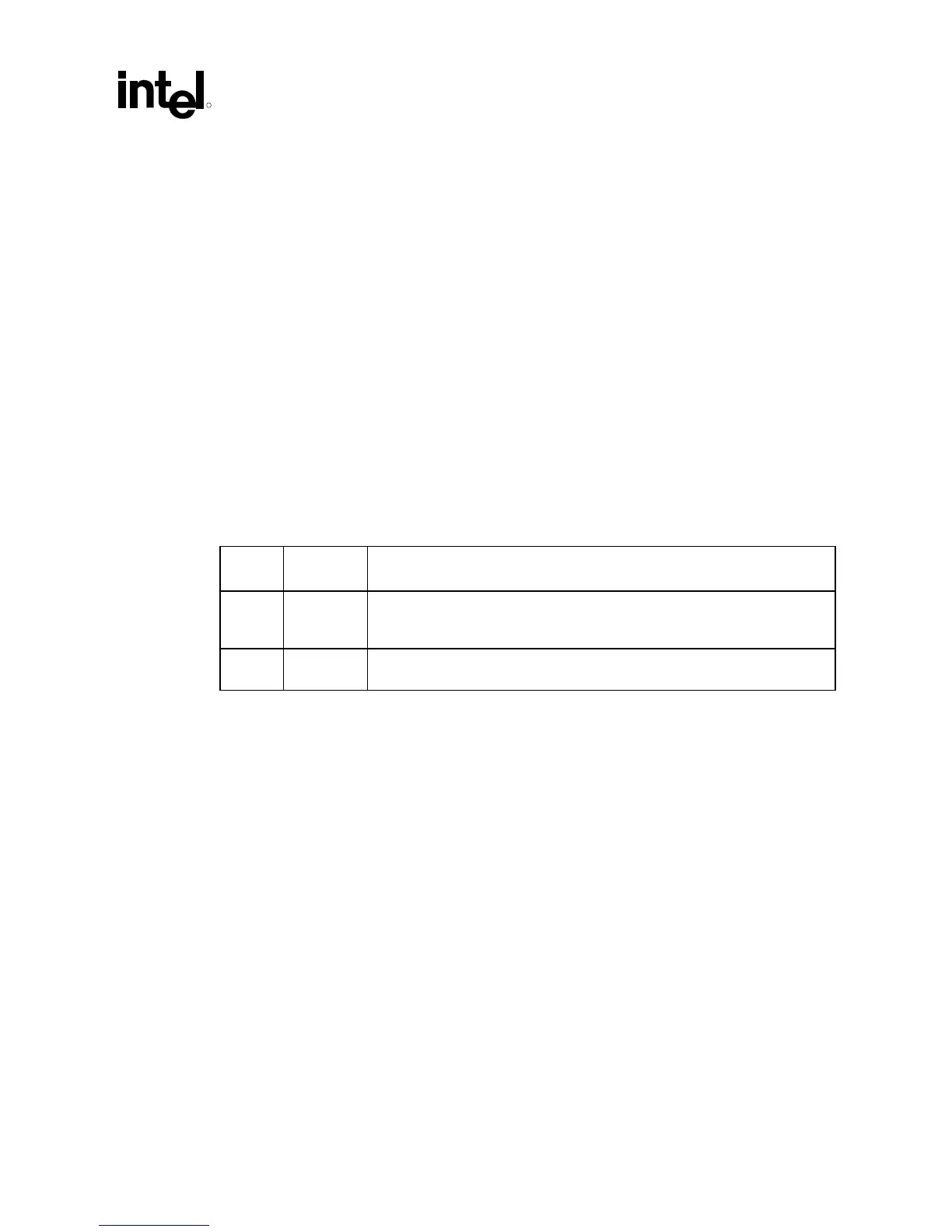
Bit Access &
Default
Description
15:4 R/W
FFFh
Prefetchable Memory Base Address (MBASE): This field corresponds to
A[31:20] of the lower limit of the memory range that will be passed to PCI
Express*.
3:0 RO
0h
64-bit Address Support: This field indicates that the bridge supports only 32 bit
addresses.
 Loading...


