Signal Description
R
30 Intel
®
82925X/82925XE MCH Datasheet
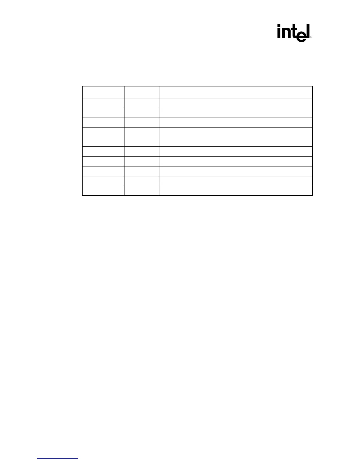
2.8 Power and Ground
Name Voltage Description
VCC 1.5 V Core Power.
VTT 1.2 V Processor System Bus Power.
VCC_EXP 1.5 V PCI Express* and DMI Power.
VCCSM 1.8 V System Memory Power.
DDR2: VCCSM = 1.8 V (VCCSM = 1.9 V for DDR2 533 CAS 3-3-3)
VCC2 2.5 V 2.5 V CMOS Power.
VCCA_EXPPLL 1.5 V PCI Express PLL Analog Power.
VCCA_HPLL 1.5 V Host PLL Analog Power.
VCCA_SMPLL 1.5 V System Memory PLL Analog Power.
VSS 0 V Ground.
2.9 Reset States and Pull-up/Pull-downs
This section describes the expected states of the MCH I/O buffers during and immediately after
the assertion of RSTIN#. This table only refers to the contributions on the interface from the
MCH and does not reflect any external influence (such as external pull-up/pull-down resistors or
external drivers).
Legend:
CMCT: Common Mode Center Tapped. Differential signals are weakly driven to the common
mode central voltage.
DRIVE: Strong drive (to normal value supplied by core logic if not otherwise stated)
TERM: Normal termination devices are turned on
LV: Low voltage
HV: High voltage
IN: Input buffer enabled
ISO: Isolate input buffer so that it does not oscillate if input left floating
TRI: Tri-state
PU: Weak internal pull-up
PD: Weak internal pull-down
STRAP: Strap input sampled during assertion or on the de-asserting edge of RSTIN#
 Loading...


