5
05.01
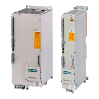
5.7 Control module ”SIMODRIVE 611 universal”
5-135
Siemens AG 2001 All rights reserved
SIMODRIVE 611 Planning Guide (PJU) – 05.01 Edition
Table 5-18 Overview of the drive–specific terminals, continued
Terminal Technical dataType
1)
Function
Drive A
Technical dataType
1)
Function
Drive B
No.
Technical dataType
1)
Function
Desig.No.Desig.
I0.A X451.7 I0.B X452.7 Digital input 0
2)
Fast input
3)
e.g. for equivalent zero
mark, external block
change
DI Voltage: 24V
Current drain, typical: 6 mA at 24 V
Signal level (including ripple)
High signal level: 15 V to 30 V
Low signal level: –3 V to 5 V
I1.A X451.8 I1.B X452.8 Digital input 1
2)
Fast input
DI
Sampling time, fast input: 62.5 µs
Electrical isolation: Reference is terminal
19/terminal M24
I2.A X451.9 I2.B X452.9 Digital input 2
2)
DI
Note:
An open input is interpreted just like a “0”
I3.A X451.10 I3.B X452.10 Digital input 3
2)
DI
An open input is interpreted just like a “0”
signal.
Drive–specific terminals (X461, X462)
X461 X462 Connector type: 10–pin, plug connector strip
Max. conductor cross–section for finely–stranded or solid conductors:
0.5 mm
2
A+.A X461.1 A+.B X462.1 Signal A+ IO Incremental shaft encoder interface
A–.A X461.2 A–.B X462.2 Signal A– IO
(WSG–SS)
Connection:
B+.A X461.3 B+.B X462.3 Signal B+ IO
Connection:
S Cable with braided shield, connected
B–.A X461.4 B–.B X462.4 Signal B– IO
at both ends.
R+.A X461.5 R+.B X462.5 Signal R+ IO
S The reference ground of the connected
node must be connected to terminal
R–.A X461.6 R–.B X462.6 Signal R– IO
X441.5.
Note:
Nodes can be connected which are in compliance with standard RS485/RS422.
The incremental shaft encoder interface can either be parameterized as input or output.
S Input To enter incremental position reference values
S Output To output incremental position actual values
O0.A X461.7 O0.B X462.7 Digital output 0
4)
DO Rated current per output: 500 mA
Maximum current per output: 600 mA
Maximum total current: 2.4 A
O1.A X461.8 O1.B X462.8 Digital output 1
4)
DO
(valid for these 8 outputs)
Typical voltage drop:
250 mV for 500 mA
O2.A X461.9 O2.B X462.9 Digital output 2
4)
DO
Short–circuit proof
Example:
The following is valid if all outputs are
simultaneously energized:
O3.A X461.10 O3.B X462.10 Digital output 3
4)
DO
simultaneously energized:
Σ current = 240 mA ––> O.K.
Σ current = 2.8 A ––> not O.K., as the total
current is greater than 2.4 A.
Note:
S The power switched via these outputs is supplied via terminals P24 / M24 (X431). When dimensioning
the external supply, this must be taken into account.
S The digital outputs only “function” if the external supply (+24 V / 0 V is available at terminals P24/M24).
1) I: Input; DO: Digital output, DI: Digital input, AO: Analog output; AI: Analog input, V: supply
2) Can be freely parameterized. All of the digital inputs are de–bounced per software. A delay time of between 1 and 2
interpolation clock cycles (P1010) is obtained due to the signal detection process.
3) I0.x is hard–wired internally for position sensing and therefore acts almost instantaneously.
4) Freely parameterizable. The digital outputs are updated in the interpolation clock cycle (P1010). A hardware–related delay
time of approx. 200 µs is involved.
5 Control Modules
 Loading...