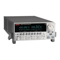
Section 6: Using a Model 82 C-V System Model 4200A-SCS Prober and External Instrument Control
6-22 4200A-913-01 Rev. A December 2020
Doping density at 90% of maximum depletion depth:
N90W = AT(NDOPING,FINDLIN(DEPTHM,0.9*MAX(DEPTHM),2))
Debye length (in meters):
DEBYEM = SQRT(ES*K*TEMP/(ABS(N90W)*Q^2))*1E-2
Flatband capacitance:
CFB = (COX*ES*AREA/(DEBYEM*1E2))/(COX+(ES*AREA/(DEBYEM*1E2)))
Flatband voltage:
VFB = AT(VGS,FINDLIN(CHADJ,CFB,2))
Bulk potential:
PHIB = (-1)*K*TEMP/Q*LN(ABS(N90W)/NI)*DOPETYPE
Threshold voltage:
VTH = VFB+DOPETYPE*(AREA/COX*SQRT(4*ES*Q*ABS(N90W*PHIB))+ 2*ABS(PHIB))
Work function difference between metal and semiconductor:
WMS = WM-(WS+(EBG/2)-PHIB)
Effective charge in oxide:
QEFF = COX*(WMS-VFB)/AREA
Index from DEPTHM array that is three Debye lengths from the surface:
BEST_LO = FINDD(DEPTHM,3*DEBYEM,2)
Index from DEPTHM array that is 95% of maximum depletion length, or twice the screening
length in the semiconductor, whichever is larger:
BEST_HI = FINDD(DEPTHM,COND(2*DEBYEM*SQRT(LN(ABS(N90W/NI))),
MAX(DEPTHM),2*DEBYEM*SQRT(LN(ABS(N90W/NI))),0.95*MAX(DEPTHM)), 2)
Average doping calculated between index BEST_HI and BEST_LO:
NAVG = AVG(SUBARRAY(NDOPING,COND(BEST_HI, BEST_LO, BEST_HI,
BEST_LO),COND(BEST_HI, BEST_LO,BEST_LO,BEST_HI)))
Interfacial states density:
DIT = 1/(AREA*Q)*(1/(1/CQADJ-1/COX)-1/(1/CHADJ-1/COX))
PSIS - PSIO, which is surface potential:
PSISPSIO = SUMMV((1-CQADJ/COX)*DELTA(VGS))*DOPETYPE
Offset in surface potential due to calculation method and flatband voltage:
PSIO = AT(PSISPSIO,FINDLIN(VGS,VFB,2))
Silicon surface potential. More precisely, this value represents band bending and is related to
surface potential via the bulk potential:
PSIS = PSISPSIO-PSIO
Interface trap energy with respect to mid band gap:
EIT = PSIS+PHIB
Formulas for ctsweep test (lifetime project)
Average doping:
NAVG = 1E15
Oxide capacitance (in picofarads):
COX = 450
Equilibrium inversion depth (in centimeters):
WF = ES*AREA*(1/MAX(CHF)-1E12/COX)
W - WF, where W is the depletion depth (in centimeters):
WWF = ES*AREA*(1/CHF-1E12/COX)-WF
Generation rate in S
-1
divided by intrinsic carrier concentration:
GNI = -(ES*AREA*NAVG*COX/1E12)*DIFF(1/CHF^2,TIME)/NI

 Loading...