Where:
• N = doping concentration (cm
-3
)
• C
Q
= quasistatic capacitance (pF)
• C
OX
= oxide capacitance (pF)
• (1-C
Q
/C
OX
)/1-C
H
/C
OX
) = voltage stretchout term
• C
H
= high-frequency capacitance (pF)
• A = gate area (cm
2
)
• q = electron charge (1.60219 × 10
-19
coulombs)
•
S
= permittivity of substrate material
• 1 × 10
-24
= units conversion factor
Interface trap density
Interface trapped charges (Q
it
) are electrons or holes trapped in localized surface states near the
Si-SiO
2
interface. These charges are one of four general types associated with the Si-SiO
2
iterface.
Interface charges interact electrically with the silicon substrate, which affects MOSFET channel
carrier mobility.
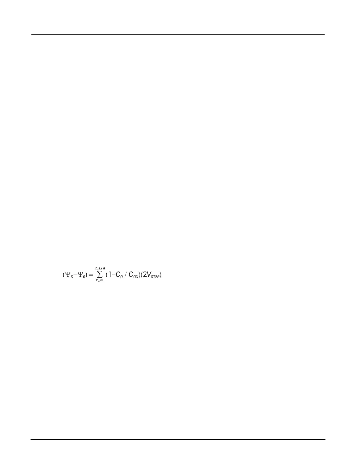
Band bending versus gate voltage
As a preliminary step, surface potential (
S
-
0
) vs. V
GS
is calculated with the results placed in the
S
column of the array. Surface potential is calculated as follows:
Where:
• (
S
-
0
) = surface potential (V)
• C
Q
= quasistatic capacitance (pF)
• C
OX
= oxide capacitance (pF)
• V
STEP
= step voltage (V)
• V
GS
= gate-substrate voltage (V)
Note that the (
S
-
0
) value is accumulated as the column is built, from the first row of the array (V
GS
#1) to the last array row (V
GS
last). The number of rows will, of course, depend on the number of
readings in the sweep, which is determined by the Start, Stop, and Step voltages.
Once (
S
-
0
) values are stored in the array, the value of (
S
-
0
) at the flatband voltage is used as a
reference point and is set to 0 by subtracting that value from each entry in the (
S
-
0
) column,
changing each element in the column to
S
.

 Loading...