Model 4200A-SCS Prober and External Instrument Control Section 6: Using a Model 82 C-V System
4200A-913-01 Rev. A December 2020 6-61
Density or concentration of interface states.
Energy of conduction band edge (valence band is E
V
).
High-frequency conductance, as measured by the Model 590 at either 100 kHz
or 1 MHz.
Bulk doping for p-type (acceptors).
Bulk doping for n-type (donors).
Average doping concentration.
Bulk doping concentration.
Effective oxide charge concentration.
Doping corresponding to 90% maximum w profile (approximates doping in the
bulk).
Mobile ion concentration in the oxide.
Current measured by the Model 595 at the end of each capacitance
measurement with the unit in the capacitance function.
Gate voltage. More specifically, the voltage at the gate with respect to the
substrate.
Flatband voltage, or the value of V
GS
that results in C
FB
.
Voltage reading sent by Model 590 with matching C
H
and G.
The point where the surface potential, S, is equal to twice the bulk
potential, B.
Depletion depth or thickness. Silicon under the gate is depleted of minority
carriers in inversion and depletion.
Silicon surface potential as a function of V
GS
. More precisely, this value
represents band bending and is related to surface potential via the bulk
potential.
Offset in S due to calculation method and V
0
.
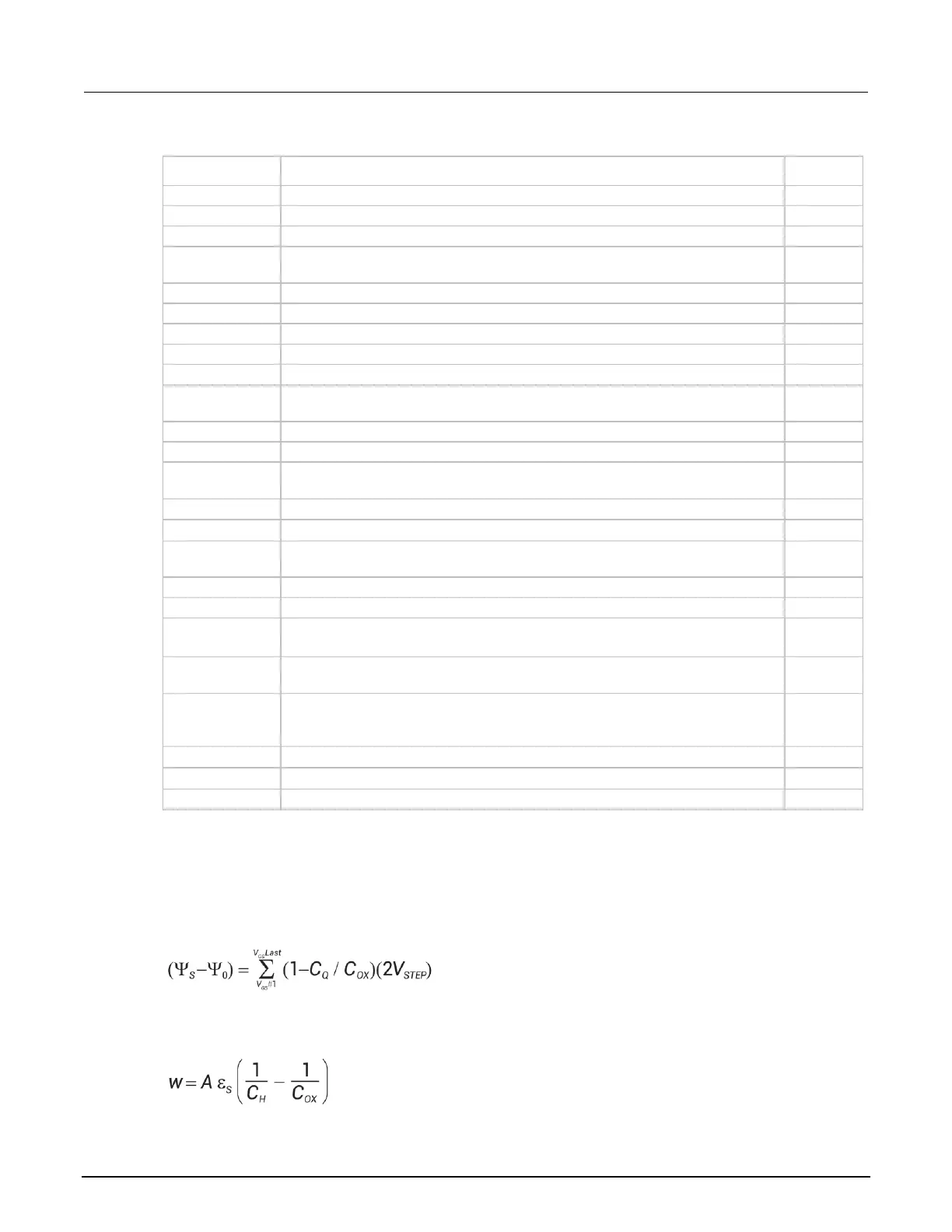
Summary of analysis equations
The analysis equations used by the Model 82 software are summarized in the following.
Band bending
Depletion depth

 Loading...